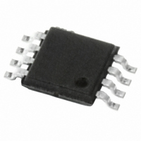
M34E02-FDW1TP STMicroelectronics, M34E02-FDW1TP Datasheet - Page 13

M34E02-FDW1TP
Manufacturer Part Number
M34E02-FDW1TP
Description
IC EEPROM 2KBIT 400KHZ 8TSSOP
Manufacturer
STMicroelectronics
Datasheet
1.M34E02-FMB1TG.pdf
(34 pages)
Specifications of M34E02-FDW1TP
Format - Memory
EEPROMs - Serial
Memory Type
EEPROM
Memory Size
2K (256 x 8)
Speed
400kHz
Interface
I²C, 2-Wire Serial
Voltage - Supply
1.7 V ~ 3.6 V
Operating Temperature
0°C ~ 70°C
Package / Case
8-TSSOP
Organization
256 K x 8
Interface Type
2-Wire
Maximum Clock Frequency
0.4 MHz
Access Time
900 ns
Supply Voltage (max)
3.6 V
Supply Voltage (min)
1.7 V
Maximum Operating Current
2 mA
Maximum Operating Temperature
+ 70 C
Mounting Style
SMD/SMT
Minimum Operating Temperature
0 C
Operating Supply Voltage
1.7 V, 3.6 V
Lead Free Status / RoHS Status
Lead free / RoHS Compliant
Other names
497-8654-2
M34E02-FDW1TP
M34E02-FDW1TP
Available stocks
Company
Part Number
Manufacturer
Quantity
Price
Company:
Part Number:
M34E02-FDW1TP
Manufacturer:
NS
Quantity:
500
Part Number:
M34E02-FDW1TP
Manufacturer:
ST
Quantity:
20 000
M34E02
3.6
3.6.1
3.6.2
Setting the write-protection
The M34E02 has a hardware write-protection feature, using the Write Control (WC) signal.
This signal can be driven high or low, and must be held constant for the whole instruction
sequence. When Write Control (WC) is held high, the whole memory array (addresses 00h
to FFh) is write protected. When Write Control (WC) is held low, the write protection of the
memory array is dependent on whether software write-protection has been set.
Software write-protection allows the bottom half of the memory area (addresses 00h to 7Fh)
to be write protected irrespective of subsequent states of the Write Control (WC) signal.
Software write-protection is handled by three instructions:
●
●
●
The level of write-protection (set or cleared) that has been defined using these instructions,
remains defined even after a power cycle.
SWP and CWP
If the software write-protection has been set with the SWP instruction, it can be cleared
again with a CWP instruction.
The two instructions (SWP and CWP) have the same format as a Byte Write instruction, but
with a different device type identifier (as shown in
is followed by an address byte and a data byte, but in this case the contents are all “Don’t
Care”
and specific logical levels must be applied on the other two (E1 and E2, as shown in
Table
PSWP
If the software write-protection has been set with the PSWP instruction, the first 128 bytes of
the memory are permanently write-protected. This write-protection cannot be cleared by
any instruction, or by power-cycling the device, and regardless the state of Write Control
(WC). Also, once the PSWP instruction has been successfully executed, the M34E02 no
longer acknowledges any instruction (with a device type identifier of 0110) to access the
write-protection settings.
Figure 7.
SWP: Set Write Protection
CWP: Clear Write Protection
PSWP: Permanently Set Write Protection
2).
(Figure
BUS ACTIVITY
MASTER
SDA LINE
BUS ACTIVITY
Setting the write protection (WC = 0)
7). Another difference is that the voltage, V
Doc ID 10367 Rev 9
CONTROL
BYTE
ACK
(DON'T CARE)
ADDRESS
VALUE
WORD
Table
ACK
2). Like the Byte Write instruction, it
(DON'T CARE)
HV
, must be applied on the E0 pin,
VALUE
DATA
AI01935B
ACK
Device operation
13/34


