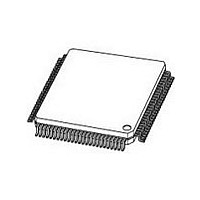
PXAH40KFBE NXP Semiconductors, PXAH40KFBE Datasheet - Page 19

PXAH40KFBE
Manufacturer Part Number
PXAH40KFBE
Description
Manufacturer
NXP Semiconductors
Datasheet
1.PXAH40KFBE.pdf
(42 pages)
Specifications of PXAH40KFBE
Cpu Family
XA
Device Core
80C51
Device Core Size
16b
Frequency (max)
30MHz
Interface Type
USART
Program Memory Type
ROMLess
Program Memory Size
Not Required
# I/os (max)
32
Number Of Timers - General Purpose
2
Operating Supply Voltage (typ)
3.3/5V
Operating Supply Voltage (max)
5.5V
Operating Supply Voltage (min)
2.97V
Instruction Set Architecture
CISC
Operating Temp Range
-40C to 85C
Operating Temperature Classification
Industrial
Mounting
Surface Mount
Pin Count
100
Package Type
LQFP
Lead Free Status / Rohs Status
Compliant
Available stocks
Company
Part Number
Manufacturer
Quantity
Price
Company:
Part Number:
PXAH40KFBE
Manufacturer:
TriQuint
Quantity:
1 200
Part Number:
PXAH40KFBE
Manufacturer:
NXP/恩智浦
Quantity:
20 000
Company:
Part Number:
PXAH40KFBE,557
Manufacturer:
NXP Semiconductors
Quantity:
10 000
Philips Semiconductors
Watchdog Timer
This timer is a standard XA-G3 Watchdog Timer. See the G3
datasheet in IC25. Also, if you intend to use the Watchdog Timer to
assert the ResetOut pin, see “ResetOut” in the XA-H4 User Manual .
The Watchdog Timer is enabled at reset, and must be periodically
fed to prevent timeout. If the watchdog times out, it will generate an
internal reset; if ResetOut is enabled, the internal reset will generate
a ResetOut pulse (active low pulse on ResetOut pin.)
Reset
On the XA-H4 there are two pins associated with reset. The ResetIn
pin provides an external reset into the XA-H4. The port pin
P3.2_Timer0_ResetOut output can be configured as ResetOut.
Because ResetOut does not reflect ResetIn, the ResetOut pin can
be tied directly back into the ResetIn pin without other PC board
logic. This configuration will make all resets (internal or external)
appear to the XA as external resets. See the XA-H4 User Manual for
a full discussion of the reset functions.
ResetIn
The ResetIn function is the standard XA-G3 ResetIn function. The
ResetIn signal does NOT get passed on to ResetOut. See the
XA-H4 User Manual for details on reset.
DRAM CONTROLLER AND MEMORY / I/O BUS
INTERFACE (MIF)
In the memory or system bus interface terminology, generic bus cycles
are synonymous with SRAM bus cycles, because these cycles are
designed to service SRAMs, Flash, EEPROM, peripheral chips, etc.
Chip select output pins function as either CS or RAS (DRAMS and
thus RAS on X-4H only) depending on whether the memory bank has
been programmed as generic or DRAM.
1999 Sep 24
Single-chip 16-bit microcontroller
RSTSRC
Not Bit Addressable
Reset Value = see below
WARNING:
If ResetOut function is tied back into ResetIn pin, RSTSRC will always show external reset ONLY, because external reset always takes
precedence over internal reset.
BIT
RSTSRC.7 ROEN
RSTSRC.6 –
RSTSRC.5 –
RSTSRC.4 –
RSTSRC.3 –
RSTSRC.2 R_WD
RSTSRC.1 R_CMD
RSTSRC.0 R_EXT
SYMBOL
Reg Type and Address = SFR 463h
MSB
ROEN
FUNCTION
ResetOut function enable bit – see XA-H3 User Manual for details
Reserved for future use. Should not be set to 1 by user programs.
Reserved for future use. Should not be set to 1 by user programs.
Reserved for future use. Should not be set to 1 by user programs.
Reserved for future use. Should not be set to 1 by user programs.
Indicates that the last reset was caused by a watchdog timer overflow (see WARNING.)
Indicates that the last reset was caused by execution of the RESET instruction (see WARNING.)
Indicates that the last reset was caused by the external ResetIn input.
—
—
Figure 2. RSTSRC reset source register
—
19
—
ResetOut
The P3.2_Timer0_ResetOut pin provides an external indication (if the
ResetOut function is enabled in the RSRSRC register) via an active
low output when an internal reset occurs (internal reset is Reset
instruction or Watchdog time out.) If the ResetOut function is enabled,
the ResetOut pin will be driven low when a Watchdog reset occurs or
the Reset instruction is executed. This signal may be used to inform
other devices in the system that the XA-H4 has been internally reset.
The ResetIn signal does NOT get passed on to ResetOut. When
activated, the duration of the ResetOut pulse is 256 system clocks.
WARNING: At power on time, from the time that power coming up is
valid, the P3.2_Timer0_ResetOut pin may be driven low for any
period from zero nanoseconds up to 258 system clocks. This is true
independently of whether ResetIn is active or not.
Reset Source Register
The Reset Source Identification Register (RSTSRC) indicates the
cause of the most recent XA reset. The cause may have been an
externally applied reset signal, execution of the RESET instruction, or
a Watchdog reset. Figure 2 shows the fields in the RSTSRC register.
If the ResetOut function is tied back into the ResetIn pin, then all
resets will be external resets, and will thus appear as external resets
in the reset source register. RSTSRC[7] enables the ResetOut
function; 1 = Enabled, 0 = Disabled. See XA-H4 User Manual for
details; RSTSRC[7] differs in function from most other XA derivatives.
The XA-H4 has a highly programmable memory bus interface with a
complete complete onboard DRAM controller. Most DRAMs (up to
8 MB per RAS pin), SRAMs, Flash, ROMs, and peripheral chips can
be connected to this interface with zero glue chips. The bus interface
provides 6 mappable chip select outputs, five of which can be
programmed to function as RAS strobes to DRAM. CAS generation,
proper address multiplexing for a wide range of DRAM sizes, and
refresh are all generated onboard. The bus timing for each individual
R_WD
R_CMD
R_EXT
LSB
Preliminary specification
XA-H4
SU01237


