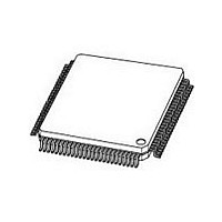
PXAH40KFBE NXP Semiconductors, PXAH40KFBE Datasheet - Page 18

PXAH40KFBE
Manufacturer Part Number
PXAH40KFBE
Description
Manufacturer
NXP Semiconductors
Datasheet
1.PXAH40KFBE.pdf
(42 pages)
Specifications of PXAH40KFBE
Cpu Family
XA
Device Core
80C51
Device Core Size
16b
Frequency (max)
30MHz
Interface Type
USART
Program Memory Type
ROMLess
Program Memory Size
Not Required
# I/os (max)
32
Number Of Timers - General Purpose
2
Operating Supply Voltage (typ)
3.3/5V
Operating Supply Voltage (max)
5.5V
Operating Supply Voltage (min)
2.97V
Instruction Set Architecture
CISC
Operating Temp Range
-40C to 85C
Operating Temperature Classification
Industrial
Mounting
Surface Mount
Pin Count
100
Package Type
LQFP
Lead Free Status / Rohs Status
Compliant
Available stocks
Company
Part Number
Manufacturer
Quantity
Price
Company:
Part Number:
PXAH40KFBE
Manufacturer:
TriQuint
Quantity:
1 200
Part Number:
PXAH40KFBE
Manufacturer:
NXP/恩智浦
Quantity:
20 000
Company:
Part Number:
PXAH40KFBE,557
Manufacturer:
NXP Semiconductors
Quantity:
10 000
Philips Semiconductors
FUNCTIONAL DESCRIPTION
The XA-H4 functions are described in the following sections.
Because all blocks are thoroughly documented in either the IC25 XA
Data Handbook , or the XA-H4 User Manual , only brief descriptions
are given in this datasheet in conjunction with references to the
appropriate document.
XA CPU
The CPU is a 30 MHz implementation of the standard XA CPU core.
See the XA Data Handbook (IC25) for details. The CPU core is
identical to the G3 core. See the caveat in the next paragraph about
the Bus Interface Unit.
Bus Interface Unit (BIU)
This is the internal Bus, not the bus at the pins. This internal bus
connects the CPU to the MIF (Memory and DRAM Controller.)
WARNING: Immediately after reset, always write BTRH = 51h,
followed by BTRL = 40h, in that order. Once written, do not change
the values in these registers. Follow these two writes with five
NOPS. Never write to the BCR register. It comes out of reset
initialized to 07h, which is the only value that will work.
1999 Sep 24
B0CFG
B0AM
B0TMG
B1CFG
B1AM
B1TMG
B2CFG
B2AM
B2TMG
B3CFG
B3AM
B3TMG
B4CFG
B4AM
B4TMG
B5CFG
B5AM
B5TMG
MBCL
RFSH
Hi-Pri Soft Ints & Pin Mux Control Reg.
XInt2
Single-chip 16-bit microcontroller
MMR Name
or Read Only
Read/Write
R/W
R/W
R/W
R/W
R/W
R/W
R/W
R/W
R/W
R/W
R/W
R/W
R/W
R/W
R/W
R/W
R/W
R/W
R/W
R/W
R/W
R/W
Memory Interface (MIF) Registers
Miscellaneous Registers
Size
16
8
8
8
8
8
8
8
8
8
8
8
8
8
8
8
8
8
8
8
8
8
Address
Offset
28Ah
28Ch
28Dh
28Eh
2BEh
2BFh
2D0h
2D2h
280h
281h
282h
284h
285h
286h
288h
289h
290h
291h
292h
294h
295h
296h
18
Timers 0 and 1
Timers 0 and 1 are the standard XA-G3 Timer 0 and 1. Each has an
associated I/O pin and interrupt. See the XA-G3 data sheet in the IC25
XA Data Handbook for details. Many XA derivatives include a standard
XA Timer 2 and standard UARTs. These blocks have been removed in
order to provide other functions on the XA-H4. There is no Timer 2 and
the UARTs have been replaced with full function USARTs.
External
Memory
and I/O Bus
MIF Bank 0 Config
MIF Bank 0 Base Address
MIF Bank 0 Timing Params
MIF Bank 1 Config
MIF Bank 1 Base Address
MIF Bank 1 Timing Params
MIF Bank 2 Config
MIF Bank 2 Base Address
MIF Bank 2 Timing Params
MIF Bank 3 Config
MIF Bank 3 Base Address
MIF Bank 3 Timing Params
MIF Bank 4 Config
MIF Bank 4 Base Address
MIF Bank 4 Timing Params
MIF Bank 5 Config
MIF Bank 5 Base Address
MIF Bank 5 Timing Params
MIF Memory Bank Configuration Lock Register
MIF Refresh Control
Control bits for Hi-Priority Soft Ints, and Pin Mux
External Interrupt 2 Control
Figure 1. XA CPU core BIU (Bus Interface Unit)
MIF and DRAM
Description
XA CPU
Controller
BIU
Internal CPU Bus
Preliminary specification
Channels
DMA
x8
XA-H4
SU01273
Reset
0Fh
00h
0000h
00h
Value


