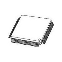
PXAH40KFBE NXP Semiconductors, PXAH40KFBE Datasheet - Page 31

PXAH40KFBE
Manufacturer Part Number
PXAH40KFBE
Description
Manufacturer
NXP Semiconductors
Datasheet
1.PXAH40KFBE.pdf
(42 pages)
Specifications of PXAH40KFBE
Cpu Family
XA
Device Core
80C51
Device Core Size
16b
Frequency (max)
30MHz
Interface Type
USART
Program Memory Type
ROMLess
Program Memory Size
Not Required
# I/os (max)
32
Number Of Timers - General Purpose
2
Operating Supply Voltage (typ)
3.3/5V
Operating Supply Voltage (max)
5.5V
Operating Supply Voltage (min)
2.97V
Instruction Set Architecture
CISC
Operating Temp Range
-40C to 85C
Operating Temperature Classification
Industrial
Mounting
Surface Mount
Pin Count
100
Package Type
LQFP
Lead Free Status / Rohs Status
Compliant
Available stocks
Company
Part Number
Manufacturer
Quantity
Price
Company:
Part Number:
PXAH40KFBE
Manufacturer:
TriQuint
Quantity:
1 200
Part Number:
PXAH40KFBE
Manufacturer:
NXP/恩智浦
Quantity:
20 000
Company:
Part Number:
PXAH40KFBE,557
Manufacturer:
NXP Semiconductors
Quantity:
10 000
8. t
9. The MIN value for this parameter is guaranteed by design and is not tested in production to the specified limit. In those cases where a
Philips Semiconductors
TIMING DIAGRAMS
All references to numbered Notes are to the notes following the AC Electrical Characteristics tables
1999 Sep 24
Single-chip 16-bit microcontroller
memory controller to service DRAM. The number of CClks (system clocks) in t
equation in the AC tables. Regardless of what value is programmed into the control register, n will never be less than 2 clocks. Thus, at
30 Mhz system clock, the minimum value for RAS precharge is tRP=((2 * t
frequency F
maximum value is specified in the table for this parameter, it is tested.
RP
Note:
is specified as the minimum high time (thus inactive) on each of the 5 individual CS_RAS[5:1] pins when such pin is programmed in the
On Generic Data Reads, A0 can terminate a full clock period before A19–A1, and therefore
should not be used on some peripheral devices.
C
, is slowed down, t
BHE/BLE
D15–D0
A19–A1
ClkOut
OE
CS
A0
Figure 7. Generic (SRAM, ROM, Flash, I/O Devices, etc.) Read on 16-Bit Bus
C
(system clock period) of course becomes greater, and thus t
t
CHAV
Note 3
t
AVSL
t
CHSL
t
DIS
31
C
) – 16= ((2 * 33.33) – 16) = 50.6 ns. As the system clock
RP
is programmable, and is represented by n in the t
t
CHSH
t
t
AHDR
DIH
(Note 2)
RP
t
CHAH
becomes greater.
(Does Not Include A0)
Preliminary specification
XA-H4
SU01277
RP


