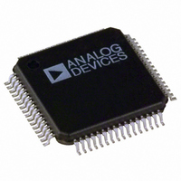
ADV7180BSTZ Analog Devices Inc, ADV7180BSTZ Datasheet - Page 60

ADV7180BSTZ
Manufacturer Part Number
ADV7180BSTZ
Description
IC VIDEO DECODER SDTV 64-LQFP
Manufacturer
Analog Devices Inc
Type
Video Decoderr
Datasheet
1.ADV7180BSTZ.pdf
(116 pages)
Specifications of ADV7180BSTZ
Design Resources
Low Cost Differential Video Receiver Using ADA4851 Amplifier and ADV7180 Video Decoder (CN0060) Low Cost Video Multiplexer for Video Switching Using ADA4853-2 Op Amp with Disable Function (CN0076)
Applications
Digital Cameras, Mobile Phones, Portable Video
Voltage - Supply, Analog
1.71 V ~ 1.89 V
Voltage - Supply, Digital
1.65 V ~ 2 V
Mounting Type
Surface Mount
Package / Case
64-LQFP
Resolution (bits)
10bit
Input Format
Analog
Output Format
Digital
Adc Sample Rate
57.27MSPS
Power Dissipation Pd
15µW
No. Of Input Channels
6
Supply Voltage Range
1.71V To 1.89V
Lead Free Status / RoHS Status
Lead free / RoHS Compliant
For Use With
EVAL-ADV7180LQEBZ - BOARD EVALUATION ADV7180EVAL-ADV7180LFEBZ - BOARD EVAL FOR ADV7180 LFCSP
Lead Free Status / RoHS Status
Lead free / RoHS Compliant, Lead free / RoHS Compliant
Available stocks
Company
Part Number
Manufacturer
Quantity
Price
Company:
Part Number:
ADV7180BSTZ
Manufacturer:
AMIS
Quantity:
6 240
Company:
Part Number:
ADV7180BSTZ
Manufacturer:
Analog Devices Inc
Quantity:
10 000
Part Number:
ADV7180BSTZ
Manufacturer:
ADI/亚德诺
Quantity:
20 000
Company:
Part Number:
ADV7180BSTZ-REEL
Manufacturer:
Analog Devices Inc
Quantity:
10 000
ADV7180
The sequence for the interrupt-based reading of the VDP I
data registers is as follows for the CCAP standard:
1.
2.
3.
4.
5.
6.
7.
Interrupt Mask Register Details
The following bits set the interrupt mask on the signal from the
VDP VBI data slicer.
VDP_CCAPD_MSK , Address 0x50[0], User Sub Map
Setting VDP_CCAPD_MSK to 0 (default) disables the interrupt
on the VDP_CCAPD_Q signal.
Setting VDP_CCAPD_MSK to 1 enables the interrupt on the
VDP_CCAPD_Q signal.
VDP_CGMS_WSS_CHNGD_MSK , Address 0x50[2], User
Sub Map
Setting VDP_CGMS_WSS_CHNGD_MSK to 0 (default) disables
the interrupt on the VDP_CGMS_WSS_ CHNGD_Q signal.
Setting VDP_CGMS_WSS_CHNGD_MSK to 1 enables the
interrupt on the VDP_CGMS_WSS_CHNGD_Q signal.
VDP_GS_VPS_PDC_UTC_CHNG_MSK ,
Address 0x50[4], User Sub Map
Setting VDP_GS_VPS_PDC_UTC_CHNG_MSK to 0
(default) disables the interrupt on the
VDP_GS_VPS_PDC_UTC_CHNG_Q signal.
Setting VDP_GS_VPS_PDC_UTC_CHNG_MSK to 1 enables
the interrupt on the VDP_GS_VPS_PDC_UTC_CHNG_Q signal.
VDP_VITC_MSK , Address 0x50[6], User Sub Map
Setting VDP_VITC_MSK to 0 (default) disables the interrupt
on the VDP_VITC_Q signal.
The user unmasks the CCAP interrupt mask bit (Register 0x50,
Bit 0, user sub map = 1). CCAP data occurs on the incoming
video. VDP slices CCAP data and places it into the VDP
readback registers.
The VDP CCAP available bit CC_CAP goes high, and the
VDP module signals to the interrupt controller to stimulate
an interrupt request (for CCAP in this case).
The user reads the interrupt status bits (user sub map) and
sees that new CCAP data is available (Register 0x4E, Bit 0,
user sub map = 1).
The user writes 1 to the CCAP interrupt clear bit (Register 0x4F,
Bit 0, user sub map = 1) in the interrupt I
self-clearing bit). This clears the interrupt on the INTRQ
pin but does not have an effect in the VDP I
The user reads the CCAP data from the VDP I
The user writes to Bit CC_CLEAR in the
VDP_STATUS_CLEAR register, (Register 0x78, Bit 0,
user sub map = 1) to signify the CCAP data has been read
(therefore the VDP CCAP can be updated at the next
occurrence of CCAP).
The user goes back to Step 2.
2
C space (this is a
2
C area.
2
C area.
2
C
Rev. F | Page 60 of 116
Setting VDP_VITC_MSK to 1 enables the interrupt on the
VDP_VITC_Q signal.
Interrupt Status Register Details
The following read-only bits contain data detection information
from the VDP module since the status bit was last cleared or
unmasked.
VDP_CCAPD_Q, Address 0x4E[0], User Sub Map
When VDP_CCAPD_Q is 0 (default), CCAP data has not been
detected.
When VDP_CCAPD_Q is 1, CCAP data has been detected.
VDP_CGMS_WSS_CHNGD_Q, Address 0x4E[2],
User Sub Map
When VDP_CGMS_WSS_CHNGD_Q is 0 (default), CGMS or
WSS data has not been detected.
When VDP_CGMS_WSS_CHNGD_Q is 1, CGM or WSS data
has been detected.
VDP_GS_VPS_PDC_UTC_CHNG_Q, Address 0x4E[4],
User Sub Map
When VDP_GS_VPS_PDC_UTC_CHNG_Q is 0 (default),
Gemstar, PDC, UTC, or VPS data has not been detected.
When VDP_GS_VPS_PDC_UTC_CHNG_Q is 1, Gemstar,
PDC, UTC, or VPS data has been detected.
VDP_VITC_Q, Address 0x4E[6], User Sub Map,
Read Only
When VDP_VITC_Q is 0 (default), VITC data has not been
detected.
When VDP_VITC_Q is 1, VITC data has been detected.
Interrupt Status Clear Register Details
It is not necessary to write 0 to these write-only bits because
they automatically reset after they have been set to 1 (self-clearing).
VDP_CCAPD_CLR, Address 0x4F[0], User Sub Map
Setting VDP_CCAPD_CLR to 1 clears the VDP_CCAP_Q bit.
VDP_CGMS_WSS_CHNGD_CLR, Address 0x4F[2],
User Sub Map
Setting VDP_CGMS_WSS_CHNGD_CLR to 1 clears the
VDP_CGMS_WSS_CHNGD_Q bit.
VDP_GS_VPS_PDC_UTC_CHNG_CLR,
Address 0x4F[4], User Sub Map
Setting VDP_GS_VPS_PDC_UTC_CHNG_CLR to 1 clears the
VDP_GS_VPS_PDC_UTC_CHNG_Q bit.
VDP_VITC_CLR, Address 0x4F[6], User Sub Map
Setting VDP_VITC_CLR to 1 clears the VDP_VITC_Q bit.


