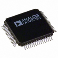
ADV7180BSTZ Analog Devices Inc, ADV7180BSTZ Datasheet - Page 56

ADV7180BSTZ
Manufacturer Part Number
ADV7180BSTZ
Description
IC VIDEO DECODER SDTV 64-LQFP
Manufacturer
Analog Devices Inc
Type
Video Decoderr
Datasheet
1.ADV7180BSTZ.pdf
(116 pages)
Specifications of ADV7180BSTZ
Design Resources
Low Cost Differential Video Receiver Using ADA4851 Amplifier and ADV7180 Video Decoder (CN0060) Low Cost Video Multiplexer for Video Switching Using ADA4853-2 Op Amp with Disable Function (CN0076)
Applications
Digital Cameras, Mobile Phones, Portable Video
Voltage - Supply, Analog
1.71 V ~ 1.89 V
Voltage - Supply, Digital
1.65 V ~ 2 V
Mounting Type
Surface Mount
Package / Case
64-LQFP
Resolution (bits)
10bit
Input Format
Analog
Output Format
Digital
Adc Sample Rate
57.27MSPS
Power Dissipation Pd
15µW
No. Of Input Channels
6
Supply Voltage Range
1.71V To 1.89V
Lead Free Status / RoHS Status
Lead free / RoHS Compliant
For Use With
EVAL-ADV7180LQEBZ - BOARD EVALUATION ADV7180EVAL-ADV7180LFEBZ - BOARD EVAL FOR ADV7180 LFCSP
Lead Free Status / RoHS Status
Lead free / RoHS Compliant, Lead free / RoHS Compliant
Available stocks
Company
Part Number
Manufacturer
Quantity
Price
Company:
Part Number:
ADV7180BSTZ
Manufacturer:
AMIS
Quantity:
6 240
Company:
Part Number:
ADV7180BSTZ
Manufacturer:
Analog Devices Inc
Quantity:
10 000
Part Number:
ADV7180BSTZ
Manufacturer:
ADI/亚德诺
Quantity:
20 000
Company:
Part Number:
ADV7180BSTZ-REEL
Manufacturer:
Analog Devices Inc
Quantity:
10 000
ADV7180
The ancillary data packet sequence is explained in Table 74 and
Table 75. The nibble output mode is the default mode of output
from the ancillary stream when ancillary stream output is
enabled. This format is in compliance with ITU-R BT.1364.
The following abbreviations are used in Table 74 and Table 75:
•
•
Table 74. Ancillary Data in Nibble Output Format
Byte
0
1
2
3
4
5
6
7
8
9
10
11
12
13
14
n − 3
n − 2
n − 1
EP—Even parity for Bit B8 to Bit B2. The parity bit’s EP is
set so that an even number of 1s are in Bit B8 to Bit B2,
including the parity bit, D8.
CS—Checksum word. The CS word is used to increase
confidence of the integrity of the ancillary data packet
from the DID, SDID, and DC through user data-words
(UDWs). It consists of 10 bits that include the following:
a 9-bit calculated value and B9 as the inverse of B8. The
checksum value B8 to B0 is equal to the nine LSBs of the
sum of the nine LSBs of the DID, SDID, and DC and all
UDWs in the packet. Prior to the start of the checksum
count cycle, all checksum and carry bits are preset to 0.
Any carry resulting from the checksum count cycle is
ignored.
B9
0
1
1
EP
EP
EP
EP
EP
EP
EP
EP
EP
EP
EP
EP
1
1
B8
B8
0
1
1
EP
EP
EP
EP
EP
EP
EP
EP
EP
EP
EP
EP
0
0
B7
0
1
1
0
0
0
EVEN_FIELD
0
0
0
0
0
0
0
0
Padding[1:0]
B6
0
1
1
0
0
0
0
0
0
0
0
Checksum (CS)
I
2
C_SDID7_2[5:0]
B5
0
1
1
0
0
0
LINE_NUMBER[9:5]
LINE_NUMBER[4:0]
Rev. F | Page 56 of 116
I
2
C_DID6_2[4:0]
B4
0
1
1
0
0
0
VBI_DATA_STD[3:0]
VBI_WORD_1[7:4]
VBI_WORD_1[3:0]
VBI_WORD_2[7:4]
VBI_WORD_2[3:0]
VBI_WORD_3[7:4]
DC[4:0]
B3
0
1
1
VDP_TTXT_TYPE[1:0]
0
0
•
•
•
EP —The MSB, B9, is the inverse of EP. This ensures that
restricted Code 0x00 and Code 0xFF do not occur.
LINE_NUMBER[9:0]—The line number of the line that
immediately precedes the ancillary data packet. The line
number is from the numbering system in ITU-R BT.470.
The line number runs from 1 to 625 in a 625-line system
and from 1 to 263 in a 525-line system. Note that, due to
the vertical delay through the comb filters, the line number
on which the packet is output differs from the line number
on which the VBI data was sliced.
Data count—The data count specifies the number of
UDWs in the ancillary stream for the standard. The total
number of user data-words is four times the data count.
Padding words can be introduced to make the total
number of UDWs divisible by 4.
B2
0
1
1
0
0
B1
0
1
1
0
0
0
0
0
0
0
0
0
0
0
0
0
0
0
0
0
0
0
B0
1
1
0
0
0
0
0
0
0
0
0
0
0
0
Description
Ancillary data preamble
DID (data identification
word)
SDID (secondary data
identification word)
Data count
ID0 (User Data-Word 1)
ID1 (User Data-Word 2)
ID2 (User Data-Word 3)
ID3 (User Data-Word 4)
ID4 (User Data-Word 5)
ID5 (User Data-Word 6)
ID6 (User Data-Word 7)
ID7 (User Data-Word 8)
ID8 (User Data-Word 9)
Pad 0x200; these
padding words may be
present, depending on
ancillary data type; user
data-word
CS (checksum word)


