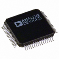
ADV7180BSTZ Analog Devices Inc, ADV7180BSTZ Datasheet - Page 19

ADV7180BSTZ
Manufacturer Part Number
ADV7180BSTZ
Description
IC VIDEO DECODER SDTV 64-LQFP
Manufacturer
Analog Devices Inc
Type
Video Decoderr
Datasheet
1.ADV7180BSTZ.pdf
(116 pages)
Specifications of ADV7180BSTZ
Design Resources
Low Cost Differential Video Receiver Using ADA4851 Amplifier and ADV7180 Video Decoder (CN0060) Low Cost Video Multiplexer for Video Switching Using ADA4853-2 Op Amp with Disable Function (CN0076)
Applications
Digital Cameras, Mobile Phones, Portable Video
Voltage - Supply, Analog
1.71 V ~ 1.89 V
Voltage - Supply, Digital
1.65 V ~ 2 V
Mounting Type
Surface Mount
Package / Case
64-LQFP
Resolution (bits)
10bit
Input Format
Analog
Output Format
Digital
Adc Sample Rate
57.27MSPS
Power Dissipation Pd
15µW
No. Of Input Channels
6
Supply Voltage Range
1.71V To 1.89V
Lead Free Status / RoHS Status
Lead free / RoHS Compliant
For Use With
EVAL-ADV7180LQEBZ - BOARD EVALUATION ADV7180EVAL-ADV7180LFEBZ - BOARD EVAL FOR ADV7180 LFCSP
Lead Free Status / RoHS Status
Lead free / RoHS Compliant, Lead free / RoHS Compliant
Available stocks
Company
Part Number
Manufacturer
Quantity
Price
Company:
Part Number:
ADV7180BSTZ
Manufacturer:
AMIS
Quantity:
6 240
Company:
Part Number:
ADV7180BSTZ
Manufacturer:
Analog Devices Inc
Quantity:
10 000
Part Number:
ADV7180BSTZ
Manufacturer:
ADI/亚德诺
Quantity:
20 000
Company:
Part Number:
ADV7180BSTZ-REEL
Manufacturer:
Analog Devices Inc
Quantity:
10 000
POWER-ON RESET
After power-up, it is necessary to execute a reset operation. For
correct operation, RESET should remain deasserted for 5 ms
after power supplies are stable and within specification and
PWRDWN (not available in 32-lead LFCSP) is asserted.
ANALOG INPUT MUXING
The ADV7180 has an integrated analog muxing section that
allows more than one source of video signal to be connected to
the decoder. Figure 12 and Figure 13 outline the overall structure of
the input muxing provided in the ADV7180.
A maximum of six CVBS inputs can be connected to and
decoded by the 64-lead and 48-lead devices, and a maximum of
three CVBS inputs can be connected to and decoded by the 40-lead
and 32-lead LFCSP devices. As shown in the Pin Configurations
and Function Description section, these analog input pins lie in
close proximity to one another, which requires careful design of
the printed circuit board (PCB) layout. For example, ground
shielding between all signals should be routed through tracks that are
physically close together. It is strongly recommended to connect
any unused analog input pins to AGND to act as a shield.
Table 15. Manual Mux Settings for the ADC (MAN_MUX_EN Must be Set to 1)
MUX0[2:0]
000
001
010
011
100
101
110
111
Note the following:
•
•
•
CVBS can only be processed by MUX0.
Y/C can only be processed by MUX0 and MUX1.
YPrPb can only be processed by MUX0, MUX1, and MUX2.
LQFP-64 or
LQFP-48
No connect
A
A
A
A
A
A
No connect
IN
IN
IN
IN
IN
IN
1
2
3
4
5
6
ADC Connected To
LFCSP-40 or
LFCSP-32
No connect
A
No connect
No connect
A
A
No connect
No connect
IN
IN
IN
1
2
3
MUX1[2:0]
001
100
101
000
010
011
110
111
Rev. F | Page 19 of 116
LQFP-64 or
LQFP-48
No connect
No connect
No connect
A
A
A
A
No connect
IN
IN
IN
IN
3
4
5
6
ADC Connected To
MAN_MUX_EN, Manual Input Muxing Enable,
Address 0xC4[7]
To configure the ADV7180 analog muxing section, the user
must select the analog input (A
and 48-lead devices or A
LFCSP devices) that is to be processed by the ADC.
MAN_MUX_EN must be set to 1 to enable the following
muxing blocks:
•
•
•
The three mux sections are controlled by the signal buses MUX0/
MUX1/MUX2[2:0]. Table 15 explains the control words used.
The input signal that contains the timing information (HS and VS)
must be processed by MUX0. For example, in a Y/C input
configuration, MUX0 should be connected to the Y channel
and MUX1 to the C channel. When one or more muxes are not
used to process video, such as the CVBS input, the idle mux and
associated channel clamps and buffers should be powered down
(see the description of Register 0x3A in Table 107).
LFCSP-40 or
LFCSP-32
No connect
No connect
No connect
No connect
A
A
No connect
No connect
MUX0[2:0], ADC Mux Configuration, Address 0xC3[2:0]
MUX1[6:4], ADC Mux Configuration, Address 0xC3[6:4]
MUX2[2:0], ADC Mux Configuration, Address 0xC4[2:0]
IN
IN
2
3
MUX2[2:0]
000
001
010
011
100
101
110
111
IN
1 to A
IN
1 to A
IN
3 for the 40-lead and 32-lead
LQFP-64 or
LQFP-48
No connect
No connect
A
No connect
No connect
A
A
No connect
IN
IN
IN
IN
6 for the 64-lead LQFP
2
5
6
ADC Connected To
ADV7180
LFCSP-40 or
LFCSP-32
No connect
No connect
No connect
No connect
No connect
A
No connect
No connect
IN
3


