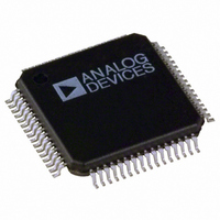
ADV7180BSTZ Analog Devices Inc, ADV7180BSTZ Datasheet - Page 29

ADV7180BSTZ
Manufacturer Part Number
ADV7180BSTZ
Description
IC VIDEO DECODER SDTV 64-LQFP
Manufacturer
Analog Devices Inc
Type
Video Decoderr
Datasheet
1.ADV7180BSTZ.pdf
(116 pages)
Specifications of ADV7180BSTZ
Design Resources
Low Cost Differential Video Receiver Using ADA4851 Amplifier and ADV7180 Video Decoder (CN0060) Low Cost Video Multiplexer for Video Switching Using ADA4853-2 Op Amp with Disable Function (CN0076)
Applications
Digital Cameras, Mobile Phones, Portable Video
Voltage - Supply, Analog
1.71 V ~ 1.89 V
Voltage - Supply, Digital
1.65 V ~ 2 V
Mounting Type
Surface Mount
Package / Case
64-LQFP
Resolution (bits)
10bit
Input Format
Analog
Output Format
Digital
Adc Sample Rate
57.27MSPS
Power Dissipation Pd
15µW
No. Of Input Channels
6
Supply Voltage Range
1.71V To 1.89V
Lead Free Status / RoHS Status
Lead free / RoHS Compliant
For Use With
EVAL-ADV7180LQEBZ - BOARD EVALUATION ADV7180EVAL-ADV7180LFEBZ - BOARD EVAL FOR ADV7180 LFCSP
Lead Free Status / RoHS Status
Lead free / RoHS Compliant, Lead free / RoHS Compliant
Available stocks
Company
Part Number
Manufacturer
Quantity
Price
Company:
Part Number:
ADV7180BSTZ
Manufacturer:
AMIS
Quantity:
6 240
Company:
Part Number:
ADV7180BSTZ
Manufacturer:
Analog Devices Inc
Quantity:
10 000
Part Number:
ADV7180BSTZ
Manufacturer:
ADI/亚德诺
Quantity:
20 000
Company:
Part Number:
ADV7180BSTZ-REEL
Manufacturer:
Analog Devices Inc
Quantity:
10 000
DEF_VAL_AUTO_EN, Default Value Automatic Enable,
Address 0x0C[1]
This bit enables the automatic use of the default values for Y, Cr,
and Cb when the ADV7180 cannot lock to the video signal.
Setting DEF_VAL_AUTO_EN to 0 disables free-run mode. If
the decoder is unlocked, it outputs noise.
Setting DEF_VAL_EN to 1 (default) enables free-run mode, and
a colored screen set by user-programmable Y, Cr, and Cb values
is displayed when the decoder loses lock.
CLAMP OPERATION
The input video is ac-coupled into the ADV7180. Therefore, its dc
value needs to be restored. This process is referred to as clamping
the video. This section explains the general process of clamping
on the ADV7180 and shows the different ways in which a user
can configure its behavior.
The ADV7180 uses a combination of current sources and a
digital processing block for clamping, as shown in Figure 20.
The analog processing channel shown is replicated three times
inside the IC. While only one single channel is needed for a
CVBS signal, two independent channels are needed for Y/C
(SVHS) type signals, and three independent channels are
needed to allow component signals (YPrPb) to be processed.
The clamping can be divided into two sections:
•
•
The ADC can digitize an input signal only if it resides within
the ADC 1.0 V input voltage range. An input signal with a dc
level that is too large or too small is clipped at the top or bottom
of the ADC range.
The primary task of the analog clamping circuits is to ensure that
the video signal stays within the valid ADC input window so that
the analog-to-digital conversion can take place. It is not necessary
to clamp the input signal with a very high accuracy in the analog
domain as long as the video signal fits within the ADC range.
Clamping before the ADC (analog domain): current
sources.
Clamping after the ADC (digital domain): digital
processing block.
FINE CURRENT SOURCES
ANALOG
VIDEO
INPUT
Figure 20. Clamping Overview
COARSE CURRENT SOURCES
Rev. F | Page 29 of 116
ADC
After digitization, the digital fine clamp block corrects for any
remaining variations in dc level. Because the dc level of an input
video signal refers directly to the brightness of the picture
transmitted, it is important to perform a fine clamp with high
accuracy; otherwise, brightness variations may occur. Further-
more, dynamic changes in the dc level almost certainly lead to
visually objectionable artifacts and must, therefore, be prohibited.
The clamping scheme has to complete two tasks. It must acquire
a newly connected video signal with a completely unknown dc
level, and it must maintain the dc level during normal operation.
To acquire an unknown video signal quickly, the large current
clamps should be activated. It is assumed that the amplitude of
the video signal at this point is of a nominal value. Control of
the coarse and fine current clamp parameters is performed
automatically by the decoder.
Standard definition video signals may have excessive noise on
them. In particular, CVBS signals transmitted by terrestrial
broadcast and demodulated using a tuner usually show very
large levels of noise (>100 mV). A voltage clamp is unsuitable
for this type of video signal. Instead, the ADV7180 employs a
set of four current sources that can cause coarse (>0.5 mA) and
fine (<0.1 mA) currents to flow into and away from the high
impedance node that carries the video signal (see Figure 20).
The following sections describe the I
to influence the behavior of the clamping block.
CCLEN, Current Clamp Enable, Address 0x14[4]
The current clamp enable bit allows the user to switch off the
current sources in the analog front end altogether. This may be
useful if the incoming analog video signal is clamped externally.
When CCLEN is 0, the current sources are switched off.
When CCLEN is 1 (default), the current sources are enabled.
PROCESSOR
CLAMP CONTROL
(DPP)
DATA
PRE-
VIDEO PROCESSOR
WITH DIGITAL
FINE CLAMP
2
C signals that can be used
ADV7180


