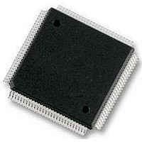
MC9S12E128CPV Freescale Semiconductor, MC9S12E128CPV Datasheet - Page 530

MC9S12E128CPV
Manufacturer Part Number
MC9S12E128CPV
Description
Microcontrollers (MCU) 16 Bit 16MHz
Manufacturer
Freescale Semiconductor
Datasheet
1.MC9S12E128CPV.pdf
(606 pages)
Specifications of MC9S12E128CPV
Data Bus Width
16 bit
Program Memory Type
Flash
Program Memory Size
128 KB
Data Ram Size
8 KB
Interface Type
SCI, SPI
Maximum Clock Frequency
25 MHz
Number Of Programmable I/os
92
Number Of Timers
16 bit
Operating Supply Voltage
3.135 V to 5.5 V
Maximum Operating Temperature
+ 85 C
Mounting Style
SMD/SMT
Package / Case
LQFP-112
Minimum Operating Temperature
- 40 C
On-chip Adc
10 bit
On-chip Dac
8 bit, 2 Channel
Lead Free Status / Rohs Status
No RoHS Version Available
Available stocks
Company
Part Number
Manufacturer
Quantity
Price
Company:
Part Number:
MC9S12E128CPVE
Manufacturer:
Freescale Semiconductor
Quantity:
10 000
- Current page: 530 of 606
- Download datasheet (4Mb)
Chapter 18 Multiplexed External Bus Interface (MEBIV3)
18.3.2.10 Pull Control Register (PUCR)
Read: Anytime (provided this register is in the map).
Write: Anytime (provided this register is in the map).
This register is used to select pull resistors for the pins associated with the core ports. Pull resistors are
assigned on a per-port basis and apply to any pin in the corresponding port that is currently configured as
an input. The polarity of these pull resistors is determined by chip integration. Please refer to the device
overview chapter to determine the polarity of these resistors.
530
MODC
a
b
0
0
0
0
1
1
1
1
Reset
No writes to the MOD bits are allowed while operating in a secure mode. For more details, refer to the device
overview chapter.
If you are in a special single-chip or special test mode and you write to this register, changing to normal sin-
gle-chip mode, then one allowed write to this register remains. If you write to normal expanded or emulation
mode, then no writes remain.
W
R
1
MODB
PUPKE
0
0
1
1
0
0
1
1
NOTES:
1. The default value of this parameter is shown. Please refer to the device overview chapter to deter-
1
7
mine the actual reset state of this register.
MODA
= Unimplemented or Reserved
0
1
0
1
0
1
0
1
Table 18-8. MODC, MODB, and MODA Write Capability
0
0
6
Figure 18-14. Pull Control Register (PUCR)
Normal expanded narrow
Normal expanded wide
Special single chip
Normal single chip
MC9S12E128 Data Sheet, Rev. 1.07
Special peripheral
Emulation narrow
Emulation wide
Special test
0
0
5
Mode
PUPEE
1
4
3
0
0
write anytime but not to 110
MODB and MODA write once
write anytime but not to 110
MODC, MODB, and MODA
MODC, MODB, and MODA
MODx Write Capability
MODC write never,
2
0
0
but not to 110
a
No write
No write
No write
No write
No write
Freescale Semiconductor
PUPBE
0
1
(2)
b
PUPAE
0
0
Related parts for MC9S12E128CPV
Image
Part Number
Description
Manufacturer
Datasheet
Request
R
Part Number:
Description:
Manufacturer:
Freescale Semiconductor, Inc
Datasheet:
Part Number:
Description:
Manufacturer:
Freescale Semiconductor, Inc
Datasheet:
Part Number:
Description:
Manufacturer:
Freescale Semiconductor, Inc
Datasheet:
Part Number:
Description:
Manufacturer:
Freescale Semiconductor, Inc
Datasheet:
Part Number:
Description:
Manufacturer:
Freescale Semiconductor, Inc
Datasheet:
Part Number:
Description:
Manufacturer:
Freescale Semiconductor, Inc
Datasheet:
Part Number:
Description:
Manufacturer:
Freescale Semiconductor, Inc
Datasheet:
Part Number:
Description:
Manufacturer:
Freescale Semiconductor, Inc
Datasheet:
Part Number:
Description:
Manufacturer:
Freescale Semiconductor, Inc
Datasheet:
Part Number:
Description:
Manufacturer:
Freescale Semiconductor, Inc
Datasheet:
Part Number:
Description:
Manufacturer:
Freescale Semiconductor, Inc
Datasheet:
Part Number:
Description:
Manufacturer:
Freescale Semiconductor, Inc
Datasheet:
Part Number:
Description:
Manufacturer:
Freescale Semiconductor, Inc
Datasheet:
Part Number:
Description:
Manufacturer:
Freescale Semiconductor, Inc
Datasheet:
Part Number:
Description:
Manufacturer:
Freescale Semiconductor, Inc
Datasheet:


