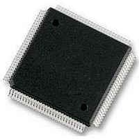
MC9S12E128CPV Freescale Semiconductor, MC9S12E128CPV Datasheet - Page 389

MC9S12E128CPV
Manufacturer Part Number
MC9S12E128CPV
Description
Microcontrollers (MCU) 16 Bit 16MHz
Manufacturer
Freescale Semiconductor
Datasheet
1.MC9S12E128CPV.pdf
(606 pages)
Specifications of MC9S12E128CPV
Data Bus Width
16 bit
Program Memory Type
Flash
Program Memory Size
128 KB
Data Ram Size
8 KB
Interface Type
SCI, SPI
Maximum Clock Frequency
25 MHz
Number Of Programmable I/os
92
Number Of Timers
16 bit
Operating Supply Voltage
3.135 V to 5.5 V
Maximum Operating Temperature
+ 85 C
Mounting Style
SMD/SMT
Package / Case
LQFP-112
Minimum Operating Temperature
- 40 C
On-chip Adc
10 bit
On-chip Dac
8 bit, 2 Channel
Lead Free Status / Rohs Status
No RoHS Version Available
Available stocks
Company
Part Number
Manufacturer
Quantity
Price
Company:
Part Number:
MC9S12E128CPVE
Manufacturer:
Freescale Semiconductor
Quantity:
10 000
- Current page: 389 of 606
- Download datasheet (4Mb)
12.3.2.3
Each PWM channel has a choice of two clocks to use as the clock source for that channel as described
below.
Read: anytime
Write: anytime
Freescale Semiconductor
PPOL2
PPOL1
PPOL0
PCLK5
PCLK4
PCLK3
Reset
Field
Field
2
1
0
5
4
3
W
R
Pulse Width Channel 2 Polarity
0 PWM channel 2 output is low at the beginning of the period, then goes high when the duty count is reached.
1 PWM channel 2 output is high at the beginning of the period, then goes low when the duty count is reached.
Pulse Width Channel 1 Polarity
0 PWM channel 1 output is low at the beginning of the period, then goes high when the duty count is reached.
1 PWM channel 1 output is high at the beginning of the period, then goes low when the duty count is reached.
Pulse Width Channel 0 Polarity
0 PWM channel 0 output is low at the beginning of the period, then goes high when the duty count is reached
1 PWM channel 0 output is high at the beginning of the period, then goes low when the duty count is reached.
Pulse Width Channel 5 Clock Select
0 Clock A is the clock source for PWM channel 5.
1 Clock SA is the clock source for PWM channel 5.
Pulse Width Channel 4 Clock Select
0 Clock A is the clock source for PWM channel 4.
1 Clock SA is the clock source for PWM channel 4.
Pulse Width Channel 3 Clock Select
0 Clock B is the clock source for PWM channel 3.
1 Clock SB is the clock source for PWM channel 3.
PWM Clock Select Register (PWMCLK)
0
0
7
Register bits PCLK0 to PCLK5 can be written anytime. If a clock select is
changed while a PWM signal is being generated, a truncated or stretched
pulse can occur during the transition.
= Unimplemented or Reserved
0
0
6
Table 12-3. PWMPOL Field Descriptions (continued)
Figure 12-5. PWM Clock Select Register (PWMCLK)
Table 12-4. PWMCLK Field Descriptions
PCLK5
MC9S12E128 Data Sheet, Rev. 1.07
0
5
PCLK4
NOTE
0
4
Description
Description
PCLK3
0
3
Chapter 12 Pulse-Width Modulator (PWM8B6CV1)
PCLK2
0
2
PCLK1
0
1
PCLK0
0
0
389
Related parts for MC9S12E128CPV
Image
Part Number
Description
Manufacturer
Datasheet
Request
R
Part Number:
Description:
Manufacturer:
Freescale Semiconductor, Inc
Datasheet:
Part Number:
Description:
Manufacturer:
Freescale Semiconductor, Inc
Datasheet:
Part Number:
Description:
Manufacturer:
Freescale Semiconductor, Inc
Datasheet:
Part Number:
Description:
Manufacturer:
Freescale Semiconductor, Inc
Datasheet:
Part Number:
Description:
Manufacturer:
Freescale Semiconductor, Inc
Datasheet:
Part Number:
Description:
Manufacturer:
Freescale Semiconductor, Inc
Datasheet:
Part Number:
Description:
Manufacturer:
Freescale Semiconductor, Inc
Datasheet:
Part Number:
Description:
Manufacturer:
Freescale Semiconductor, Inc
Datasheet:
Part Number:
Description:
Manufacturer:
Freescale Semiconductor, Inc
Datasheet:
Part Number:
Description:
Manufacturer:
Freescale Semiconductor, Inc
Datasheet:
Part Number:
Description:
Manufacturer:
Freescale Semiconductor, Inc
Datasheet:
Part Number:
Description:
Manufacturer:
Freescale Semiconductor, Inc
Datasheet:
Part Number:
Description:
Manufacturer:
Freescale Semiconductor, Inc
Datasheet:
Part Number:
Description:
Manufacturer:
Freescale Semiconductor, Inc
Datasheet:
Part Number:
Description:
Manufacturer:
Freescale Semiconductor, Inc
Datasheet:


