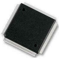
MC9S12E128CPV Freescale Semiconductor, MC9S12E128CPV Datasheet - Page 475

MC9S12E128CPV
Manufacturer Part Number
MC9S12E128CPV
Description
Microcontrollers (MCU) 16 Bit 16MHz
Manufacturer
Freescale Semiconductor
Datasheet
1.MC9S12E128CPV.pdf
(606 pages)
Specifications of MC9S12E128CPV
Data Bus Width
16 bit
Program Memory Type
Flash
Program Memory Size
128 KB
Data Ram Size
8 KB
Interface Type
SCI, SPI
Maximum Clock Frequency
25 MHz
Number Of Programmable I/os
92
Number Of Timers
16 bit
Operating Supply Voltage
3.135 V to 5.5 V
Maximum Operating Temperature
+ 85 C
Mounting Style
SMD/SMT
Package / Case
LQFP-112
Minimum Operating Temperature
- 40 C
On-chip Adc
10 bit
On-chip Dac
8 bit, 2 Channel
Lead Free Status / Rohs Status
No RoHS Version Available
Available stocks
Company
Part Number
Manufacturer
Quantity
Price
Company:
Part Number:
MC9S12E128CPVE
Manufacturer:
Freescale Semiconductor
Quantity:
10 000
- Current page: 475 of 606
- Download datasheet (4Mb)
16.1.2
There are two main modes of operation: breakpoint mode and debug mode. Each one is mutually exclusive
of the other and selected via a software programmable control bit.
In the breakpoint mode there are two sub-modes of operation:
In debug mode, there are several sub-modes of operation.
16.1.3
Figure 16-1
module in debug mode.
Freescale Semiconductor
•
•
•
•
— Data associated with event B trigger modes
— Detail report mode stores address and data for all cycles except program (P) and free (f) cycles
— Current instruction address when in profiling mode
— BGND is not considered a change-of-flow (cof) by the debugger
Dual address mode, where a match on either of two addresses will cause the system to enter
background debug mode (BDM) or initiate a software interrupt (SWI).
Full breakpoint mode, where a match on address and data will cause the system to enter
background debug mode (BDM) or initiate a software interrupt (SWI).
Trigger modes
There are many ways to create a logical trigger. The trigger can be used to capture bus information
either starting from the trigger or ending at the trigger. Types of triggers (A and B are registers):
— A only
— A or B
— A then B
— Event only B (data capture)
— A then event only B (data capture)
— A and B, full mode
— A and not B, full mode
— Inside range
— Outside range
Capture modes
There are several capture modes. These determine which bus information is saved and which is
ignored.
— Normal: save change-of-flow program fetches
— Loop1: save change-of-flow program fetches, ignoring duplicates
— Detail: save all bus operations except program and free cycles
— Profile: poll target from external device
Modes of Operation
Block Diagram
is a block diagram of this module in breakpoint mode.
MC9S12E128 Data Sheet, Rev. 1.07
Figure 16-2
Chapter 16 Debug Module (DBGV1)
is a block diagram of this
475
Related parts for MC9S12E128CPV
Image
Part Number
Description
Manufacturer
Datasheet
Request
R
Part Number:
Description:
Manufacturer:
Freescale Semiconductor, Inc
Datasheet:
Part Number:
Description:
Manufacturer:
Freescale Semiconductor, Inc
Datasheet:
Part Number:
Description:
Manufacturer:
Freescale Semiconductor, Inc
Datasheet:
Part Number:
Description:
Manufacturer:
Freescale Semiconductor, Inc
Datasheet:
Part Number:
Description:
Manufacturer:
Freescale Semiconductor, Inc
Datasheet:
Part Number:
Description:
Manufacturer:
Freescale Semiconductor, Inc
Datasheet:
Part Number:
Description:
Manufacturer:
Freescale Semiconductor, Inc
Datasheet:
Part Number:
Description:
Manufacturer:
Freescale Semiconductor, Inc
Datasheet:
Part Number:
Description:
Manufacturer:
Freescale Semiconductor, Inc
Datasheet:
Part Number:
Description:
Manufacturer:
Freescale Semiconductor, Inc
Datasheet:
Part Number:
Description:
Manufacturer:
Freescale Semiconductor, Inc
Datasheet:
Part Number:
Description:
Manufacturer:
Freescale Semiconductor, Inc
Datasheet:
Part Number:
Description:
Manufacturer:
Freescale Semiconductor, Inc
Datasheet:
Part Number:
Description:
Manufacturer:
Freescale Semiconductor, Inc
Datasheet:
Part Number:
Description:
Manufacturer:
Freescale Semiconductor, Inc
Datasheet:


