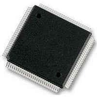
MC9S12E128CPV Freescale Semiconductor, MC9S12E128CPV Datasheet - Page 407

MC9S12E128CPV
Manufacturer Part Number
MC9S12E128CPV
Description
Microcontrollers (MCU) 16 Bit 16MHz
Manufacturer
Freescale Semiconductor
Datasheet
1.MC9S12E128CPV.pdf
(606 pages)
Specifications of MC9S12E128CPV
Data Bus Width
16 bit
Program Memory Type
Flash
Program Memory Size
128 KB
Data Ram Size
8 KB
Interface Type
SCI, SPI
Maximum Clock Frequency
25 MHz
Number Of Programmable I/os
92
Number Of Timers
16 bit
Operating Supply Voltage
3.135 V to 5.5 V
Maximum Operating Temperature
+ 85 C
Mounting Style
SMD/SMT
Package / Case
LQFP-112
Minimum Operating Temperature
- 40 C
On-chip Adc
10 bit
On-chip Dac
8 bit, 2 Channel
Lead Free Status / Rohs Status
No RoHS Version Available
Available stocks
Company
Part Number
Manufacturer
Quantity
Price
Company:
Part Number:
MC9S12E128CPVE
Manufacturer:
Freescale Semiconductor
Quantity:
10 000
- Current page: 407 of 606
- Download datasheet (4Mb)
12.4.2.1
Each PWM channel has an enable bit (PWMEx) to start its waveform output. When any of the PWMEx
bits are set (PWMEx = 1), the associated PWM output signal is enabled immediately. However, the actual
PWM waveform is not available on the associated PWM output until its clock source begins its next cycle
due to the synchronization of PWMEx and the clock source. An exception to this is when channels are
concatenated. Refer to
On the front end of the PWM timer, the clock is enabled to the PWM circuit by the PWMEx bit being high.
There is an edge-synchronizing circuit to guarantee that the clock will only be enabled or disabled at an
edge. When the channel is disabled (PWMEx = 0), the counter for the channel does not count.
12.4.2.2
Each channel has a polarity bit to allow starting a waveform cycle with a high or low signal. This is shown
on the block diagram as a mux select of either the Q output or the Q output of the PWM output flip-flop.
When one of the bits in the PWMPOL register is set, the associated PWM channel output is high at the
beginning of the waveform, then goes low when the duty count is reached. Conversely, if the polarity bit
is 0, the output starts low and then goes high when the duty count is reached.
12.4.2.3
Dedicated period and duty registers exist for each channel and are double buffered so that if they change
while the channel is enabled, the change will NOT take effect until one of the following occurs:
In this way, the output of the PWM will always be either the old waveform or the new waveform, not some
variation in between. If the channel is not enabled, then writes to the period and duty registers will go
directly to the latches as well as the buffer.
A change in duty or period can be forced into effect “immediately” by writing the new value to the duty
and/or period registers and then writing to the counter. This forces the counter to reset and the new duty
and/or period values to be latched. In addition, because the counter is readable it is possible to know where
the count is with respect to the duty value and software can be used to make adjustments.
Freescale Semiconductor
•
•
•
The effective period ends
The counter is written (counter resets to 0x0000)
The channel is disabled
PWM Enable
PWM Polarity
PWM Period and Duty
The first PWM cycle after enabling the channel can be irregular.
When forcing a new period or duty into effect immediately, an irregular
PWM cycle can occur.
Depending on the polarity bit, the duty registers will contain the count of
either the high time or the low time.
Section 12.4.2.7, “PWM 16-Bit Functions,”
MC9S12E128 Data Sheet, Rev. 1.07
NOTE
NOTE
Chapter 12 Pulse-Width Modulator (PWM8B6CV1)
for more detail.
407
Related parts for MC9S12E128CPV
Image
Part Number
Description
Manufacturer
Datasheet
Request
R
Part Number:
Description:
Manufacturer:
Freescale Semiconductor, Inc
Datasheet:
Part Number:
Description:
Manufacturer:
Freescale Semiconductor, Inc
Datasheet:
Part Number:
Description:
Manufacturer:
Freescale Semiconductor, Inc
Datasheet:
Part Number:
Description:
Manufacturer:
Freescale Semiconductor, Inc
Datasheet:
Part Number:
Description:
Manufacturer:
Freescale Semiconductor, Inc
Datasheet:
Part Number:
Description:
Manufacturer:
Freescale Semiconductor, Inc
Datasheet:
Part Number:
Description:
Manufacturer:
Freescale Semiconductor, Inc
Datasheet:
Part Number:
Description:
Manufacturer:
Freescale Semiconductor, Inc
Datasheet:
Part Number:
Description:
Manufacturer:
Freescale Semiconductor, Inc
Datasheet:
Part Number:
Description:
Manufacturer:
Freescale Semiconductor, Inc
Datasheet:
Part Number:
Description:
Manufacturer:
Freescale Semiconductor, Inc
Datasheet:
Part Number:
Description:
Manufacturer:
Freescale Semiconductor, Inc
Datasheet:
Part Number:
Description:
Manufacturer:
Freescale Semiconductor, Inc
Datasheet:
Part Number:
Description:
Manufacturer:
Freescale Semiconductor, Inc
Datasheet:
Part Number:
Description:
Manufacturer:
Freescale Semiconductor, Inc
Datasheet:


