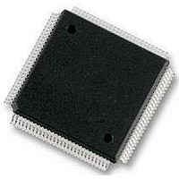
MC9S12E128CPV Freescale Semiconductor, MC9S12E128CPV Datasheet - Page 365

MC9S12E128CPV
Manufacturer Part Number
MC9S12E128CPV
Description
Microcontrollers (MCU) 16 Bit 16MHz
Manufacturer
Freescale Semiconductor
Datasheet
1.MC9S12E128CPV.pdf
(606 pages)
Specifications of MC9S12E128CPV
Data Bus Width
16 bit
Program Memory Type
Flash
Program Memory Size
128 KB
Data Ram Size
8 KB
Interface Type
SCI, SPI
Maximum Clock Frequency
25 MHz
Number Of Programmable I/os
92
Number Of Timers
16 bit
Operating Supply Voltage
3.135 V to 5.5 V
Maximum Operating Temperature
+ 85 C
Mounting Style
SMD/SMT
Package / Case
LQFP-112
Minimum Operating Temperature
- 40 C
On-chip Adc
10 bit
On-chip Dac
8 bit, 2 Channel
Lead Free Status / Rohs Status
No RoHS Version Available
Available stocks
Company
Part Number
Manufacturer
Quantity
Price
Company:
Part Number:
MC9S12E128CPVE
Manufacturer:
Freescale Semiconductor
Quantity:
10 000
- Current page: 365 of 606
- Download datasheet (4Mb)
For a given PWM pair, whether the odd or even PMFVAL register is active depends on either:
To correct deadtime distortion, software can decrease or increase the value in the appropriate PMFVAL
register.
In the complementary channel operation, ISENS selects one of three correction methods:
Freescale Semiconductor
•
•
•
•
•
•
•
The state of the current status pin, ISx, for that driver
The state of the odd/even correction bit, IPOLx, for that driver
In edge-aligned operation, decreasing or increasing the PWM value by a correction value equal to
the deadtime typically compensates for deadtime distortion.
In center-aligned operation, decreasing or increasing the PWM value by a correction value equal
to one-half the deadtime typically compensates for deadtime distortion.
Manual correction
Automatic current status correction during deadtime
Automatic current status correction when the PWM counter value equals the value in the PWM
counter modulus registers
1
2
3
Assume the user will provide current status sensing circuitry causing the
voltage at the corresponding input pin to be low for positive current and high
for negative current. In addition, it assumes the top PWMs are PWM 0, 2,
and 4 while the bottom PWMS are PWM 1, 3, and 5.
The current status pins can be used as general purpose input/output ports.
The polarity of the ISx pin is latched when both the top and bottom PWMs are off. At the 0%
and 100% duty cycle boundaries, there is no deadtime, so no new current value is sensed.
Current is sensed even with 0% or 100% duty cycle.
ISENS
00
01
10
11
No correction
Manual correction
Current status sample correction on pins IS0, IS1, and IS2 during deadtime
Current status sample on pins IS0, IS1, and IS2
At the half cycle in center-aligned operation
At the end of the cycle in edge-aligned operation
Table 11-47. Correction Method Selection
MC9S12E128 Data Sheet, Rev. 1.07
1
Chapter 11 Pulse Width Modulator with Fault Protection (PMF15B6CV2)
NOTE
Correction Method
3
2
365
Related parts for MC9S12E128CPV
Image
Part Number
Description
Manufacturer
Datasheet
Request
R
Part Number:
Description:
Manufacturer:
Freescale Semiconductor, Inc
Datasheet:
Part Number:
Description:
Manufacturer:
Freescale Semiconductor, Inc
Datasheet:
Part Number:
Description:
Manufacturer:
Freescale Semiconductor, Inc
Datasheet:
Part Number:
Description:
Manufacturer:
Freescale Semiconductor, Inc
Datasheet:
Part Number:
Description:
Manufacturer:
Freescale Semiconductor, Inc
Datasheet:
Part Number:
Description:
Manufacturer:
Freescale Semiconductor, Inc
Datasheet:
Part Number:
Description:
Manufacturer:
Freescale Semiconductor, Inc
Datasheet:
Part Number:
Description:
Manufacturer:
Freescale Semiconductor, Inc
Datasheet:
Part Number:
Description:
Manufacturer:
Freescale Semiconductor, Inc
Datasheet:
Part Number:
Description:
Manufacturer:
Freescale Semiconductor, Inc
Datasheet:
Part Number:
Description:
Manufacturer:
Freescale Semiconductor, Inc
Datasheet:
Part Number:
Description:
Manufacturer:
Freescale Semiconductor, Inc
Datasheet:
Part Number:
Description:
Manufacturer:
Freescale Semiconductor, Inc
Datasheet:
Part Number:
Description:
Manufacturer:
Freescale Semiconductor, Inc
Datasheet:
Part Number:
Description:
Manufacturer:
Freescale Semiconductor, Inc
Datasheet:


