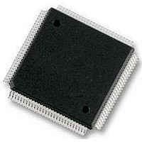
MC9S12E128CPV Freescale Semiconductor, MC9S12E128CPV Datasheet - Page 377

MC9S12E128CPV
Manufacturer Part Number
MC9S12E128CPV
Description
Microcontrollers (MCU) 16 Bit 16MHz
Manufacturer
Freescale Semiconductor
Datasheet
1.MC9S12E128CPV.pdf
(606 pages)
Specifications of MC9S12E128CPV
Data Bus Width
16 bit
Program Memory Type
Flash
Program Memory Size
128 KB
Data Ram Size
8 KB
Interface Type
SCI, SPI
Maximum Clock Frequency
25 MHz
Number Of Programmable I/os
92
Number Of Timers
16 bit
Operating Supply Voltage
3.135 V to 5.5 V
Maximum Operating Temperature
+ 85 C
Mounting Style
SMD/SMT
Package / Case
LQFP-112
Minimum Operating Temperature
- 40 C
On-chip Adc
10 bit
On-chip Dac
8 bit, 2 Channel
Lead Free Status / Rohs Status
No RoHS Version Available
Available stocks
Company
Part Number
Manufacturer
Quantity
Price
Company:
Part Number:
MC9S12E128CPVE
Manufacturer:
Freescale Semiconductor
Quantity:
10 000
- Current page: 377 of 606
- Download datasheet (4Mb)
When the PWMEN bit is cleared:
11.4.8
Fault protection can disable any combination of PWM pins. Faults are generated by a logic one on any of
the FAULT pins. Each FAULT pin can be mapped arbitrarily to any of the PWM pins.
When fault protection hardware disables PWM pins, the PWM generator continues to run, only the output
pins are deactivated.
The fault decoder disables PWM pins selected by the fault logic and the disable mapping register. See
Figure
pin. Refer to
The fault protection is enabled even when the PWM is not enabled; therefore, a fault will be latched in and
will be cleared in order to prevent an interrupt when the PWM is enabled.
11.4.8.1
Each fault pin has a sample filter to test for fault conditions. After every bus cycle setting the FAULTx pin
at logic zero, the filter synchronously samples the pin once every four bus cycles. QSMP determines the
number of consecutive samples that must be logic one for a fault to be detected. When a fault is detected,
the corresponding FAULTx pin flag, FFLAGx, is set. Clear FFLAGx by writing a logic one to it.
If the FIEx, FAULTx pin interrupt enable bit is set, the FFLAGx flag generates a CPU interrupt request.
The interrupt request latch remains set until:
Freescale Semiconductor
•
•
•
•
•
•
•
•
•
•
11-15. Each bank of four bits in the disable mapping register control the mapping for a single PWM
The PWMx outputs will be tri-stated unless OUTCTLx = 1
The PWM counter is cleared and does not count
The PWM generator forces its outputs to zero
The PWMRF flag and pending CPU interrupt requests are not cleared
All fault circuitry remains active unless FPINEx = 0
Software output control remains active
Deadtime insertion continues during software output control
Software clears the FFLAGx flag by writing a logic one to it
Software clears the FIEx bit by writing a logic zero to it
A reset occurs
Fault Protection
Table
Fault Pin Sample Filter
11-12.
MC9S12E128 Data Sheet, Rev. 1.07
Chapter 11 Pulse Width Modulator with Fault Protection (PMF15B6CV2)
377
Related parts for MC9S12E128CPV
Image
Part Number
Description
Manufacturer
Datasheet
Request
R
Part Number:
Description:
Manufacturer:
Freescale Semiconductor, Inc
Datasheet:
Part Number:
Description:
Manufacturer:
Freescale Semiconductor, Inc
Datasheet:
Part Number:
Description:
Manufacturer:
Freescale Semiconductor, Inc
Datasheet:
Part Number:
Description:
Manufacturer:
Freescale Semiconductor, Inc
Datasheet:
Part Number:
Description:
Manufacturer:
Freescale Semiconductor, Inc
Datasheet:
Part Number:
Description:
Manufacturer:
Freescale Semiconductor, Inc
Datasheet:
Part Number:
Description:
Manufacturer:
Freescale Semiconductor, Inc
Datasheet:
Part Number:
Description:
Manufacturer:
Freescale Semiconductor, Inc
Datasheet:
Part Number:
Description:
Manufacturer:
Freescale Semiconductor, Inc
Datasheet:
Part Number:
Description:
Manufacturer:
Freescale Semiconductor, Inc
Datasheet:
Part Number:
Description:
Manufacturer:
Freescale Semiconductor, Inc
Datasheet:
Part Number:
Description:
Manufacturer:
Freescale Semiconductor, Inc
Datasheet:
Part Number:
Description:
Manufacturer:
Freescale Semiconductor, Inc
Datasheet:
Part Number:
Description:
Manufacturer:
Freescale Semiconductor, Inc
Datasheet:
Part Number:
Description:
Manufacturer:
Freescale Semiconductor, Inc
Datasheet:


