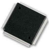
MC9S12E128CPV Freescale Semiconductor, MC9S12E128CPV Datasheet - Page 517

MC9S12E128CPV
Manufacturer Part Number
MC9S12E128CPV
Description
Microcontrollers (MCU) 16 Bit 16MHz
Manufacturer
Freescale Semiconductor
Datasheet
1.MC9S12E128CPV.pdf
(606 pages)
Specifications of MC9S12E128CPV
Data Bus Width
16 bit
Program Memory Type
Flash
Program Memory Size
128 KB
Data Ram Size
8 KB
Interface Type
SCI, SPI
Maximum Clock Frequency
25 MHz
Number Of Programmable I/os
92
Number Of Timers
16 bit
Operating Supply Voltage
3.135 V to 5.5 V
Maximum Operating Temperature
+ 85 C
Mounting Style
SMD/SMT
Package / Case
LQFP-112
Minimum Operating Temperature
- 40 C
On-chip Adc
10 bit
On-chip Dac
8 bit, 2 Channel
Lead Free Status / Rohs Status
No RoHS Version Available
Available stocks
Company
Part Number
Manufacturer
Quantity
Price
Company:
Part Number:
MC9S12E128CPVE
Manufacturer:
Freescale Semiconductor
Quantity:
10 000
- Current page: 517 of 606
- Download datasheet (4Mb)
Detailed descriptions of these pins can be found in the device overview chapter.
Freescale Semiconductor
PE5/IPIPE0/MODA
PE4/ECLK
PE3/LSTRB/ TAGLO
PE2/R/W
PE1/IRQ
PE0/XIRQ
PK7/ECS
PK6/XCS
PK5/X19
thru
PK0/X14
Pin Name
Table 18-1. External System Pins Associated With MEBI (continued)
MODA
PE5
IPIPE0
PE4
ECLK
PE3
LSTRB
SZ8
TAGLO
PE2
R/W
PE1
IRQ
PE0
XIRQ
PK7
ECS
PK6
XCS
PK5–PK0
X19–X14
Pin Functions
MC9S12E128 Data Sheet, Rev. 1.07
At the rising edge on RESET, the state of this pin is registered into the MODA
bit to set the mode.
General-purpose I/O pin, see PORTE and DDRE registers.
Instruction pipe status bit 0, enabled by PIPOE bit in PEAR.
General-purpose I/O pin, see PORTE and DDRE registers.
Bus timing reference clock, can operate as a free-running clock at the system
clock rate or to produce one low-high clock per visible access, with the high
period stretched for slow accesses. ECLK is controlled by the NECLK bit in
PEAR, the IVIS bit in MODE, and the ESTR bit in EBICTL.
General-purpose I/O pin, see PORTE and DDRE registers.
Low strobe bar, 0 indicates valid data on D7–D0.
In special peripheral mode, this pin is an input indicating the size of the data
transfer (0 = 16-bit; 1 = 8-bit).
In expanded wide mode or emulation narrow modes, when instruction tagging
is on and low strobe is enabled, a 0 at the falling edge of E tags the low half of
the instruction word being read into the instruction queue.
General-purpose I/O pin, see PORTE and DDRE registers.
Read/write, indicates the direction of internal data transfers. This is an output
except in special peripheral mode where it is an input.
General-purpose input-only pin, can be read even if IRQ enabled.
Maskable interrupt request, can be level sensitive or edge sensitive.
General-purpose input-only pin.
Non-maskable interrupt input.
General-purpose I/O pin, see PORTK and DDRK registers.
Emulation chip select
General-purpose I/O pin, see PORTK and DDRK registers.
External data chip select
General-purpose I/O pins, see PORTK and DDRK registers.
Memory expansion addresses
Chapter 18 Multiplexed External Bus Interface (MEBIV3)
Description
517
Related parts for MC9S12E128CPV
Image
Part Number
Description
Manufacturer
Datasheet
Request
R
Part Number:
Description:
Manufacturer:
Freescale Semiconductor, Inc
Datasheet:
Part Number:
Description:
Manufacturer:
Freescale Semiconductor, Inc
Datasheet:
Part Number:
Description:
Manufacturer:
Freescale Semiconductor, Inc
Datasheet:
Part Number:
Description:
Manufacturer:
Freescale Semiconductor, Inc
Datasheet:
Part Number:
Description:
Manufacturer:
Freescale Semiconductor, Inc
Datasheet:
Part Number:
Description:
Manufacturer:
Freescale Semiconductor, Inc
Datasheet:
Part Number:
Description:
Manufacturer:
Freescale Semiconductor, Inc
Datasheet:
Part Number:
Description:
Manufacturer:
Freescale Semiconductor, Inc
Datasheet:
Part Number:
Description:
Manufacturer:
Freescale Semiconductor, Inc
Datasheet:
Part Number:
Description:
Manufacturer:
Freescale Semiconductor, Inc
Datasheet:
Part Number:
Description:
Manufacturer:
Freescale Semiconductor, Inc
Datasheet:
Part Number:
Description:
Manufacturer:
Freescale Semiconductor, Inc
Datasheet:
Part Number:
Description:
Manufacturer:
Freescale Semiconductor, Inc
Datasheet:
Part Number:
Description:
Manufacturer:
Freescale Semiconductor, Inc
Datasheet:
Part Number:
Description:
Manufacturer:
Freescale Semiconductor, Inc
Datasheet:


