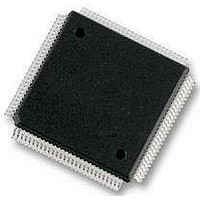
MC9S12E128CPV Freescale Semiconductor, MC9S12E128CPV Datasheet - Page 405

MC9S12E128CPV
Manufacturer Part Number
MC9S12E128CPV
Description
Microcontrollers (MCU) 16 Bit 16MHz
Manufacturer
Freescale Semiconductor
Datasheet
1.MC9S12E128CPV.pdf
(606 pages)
Specifications of MC9S12E128CPV
Data Bus Width
16 bit
Program Memory Type
Flash
Program Memory Size
128 KB
Data Ram Size
8 KB
Interface Type
SCI, SPI
Maximum Clock Frequency
25 MHz
Number Of Programmable I/os
92
Number Of Timers
16 bit
Operating Supply Voltage
3.135 V to 5.5 V
Maximum Operating Temperature
+ 85 C
Mounting Style
SMD/SMT
Package / Case
LQFP-112
Minimum Operating Temperature
- 40 C
On-chip Adc
10 bit
On-chip Dac
8 bit, 2 Channel
Lead Free Status / Rohs Status
No RoHS Version Available
Available stocks
Company
Part Number
Manufacturer
Quantity
Price
Company:
Part Number:
MC9S12E128CPVE
Manufacturer:
Freescale Semiconductor
Quantity:
10 000
- Current page: 405 of 606
- Download datasheet (4Mb)
12.4.1.2
The scaled A clock uses clock A as an input and divides it further with a user programmable value and
then divides this by 2. The scaled B clock uses clock B as an input and divides it further with a user
programmable value and then divides this by 2. The rates available for clock SA are software selectable
to be clock A divided by 2, 4, 6, 8, ..., or 512 in increments of divide by 2. Similar rates are available for
clock SB.
Clock A is used as an input to an 8-bit down counter. This down counter loads a user programmable scale
value from the scale register (PWMSCLA). When the down counter reaches 1, two things happen; a pulse
is output and the 8-bit counter is re-loaded. The output signal from this circuit is further divided by two.
This gives a greater range with only a slight reduction in granularity. Clock SA equals clock A divided by
two times the value in the PWMSCLA register.
Similarly, clock B is used as an input to an 8-bit down counter followed by a divide by two producing clock
SB. Thus, clock SB equals clock B divided by two times the value in the PWMSCLB register.
As an example, consider the case in which the user writes 0x00FF into the PWMSCLA register. Clock A
for this case will be bus clock divided by 4. A pulse will occur at a rate of once every 255 x 4 bus cycles.
Passing this through the divide by two circuit produces a clock signal at a bus clock divided by 2040 rate.
Similarly, a value of 0x0001 in the PWMSCLA register when clock A is bus clock divided by 4 will
produce a bus clock divided by 8 rate.
Writing to PWMSCLA or PWMSCLB causes the associated 8-bit down counter to be re-loaded.
Otherwise, when changing rates the counter would have to count down to 0x0001 before counting at the
proper rate. Forcing the associated counter to re-load the scale register value every time PWMSCLA or
PWMSCLB is written prevents this.
Freescale Semiconductor
Clock Scale
Clock SA = Clock A / (2 * PWMSCLA)
When PWMSCLA = 0x0000, PWMSCLA value is considered a full scale
value of 256. Clock A is thus divided by 512.
Clock SB = Clock B / (2 * PWMSCLB)
When PWMSCLB = 0x0000, PWMSCLB value is considered a full scale
value of 256. Clock B is thus divided by 512.
Writing to the scale registers while channels are operating can cause
irregularities in the PWM outputs.
MC9S12E128 Data Sheet, Rev. 1.07
NOTE
NOTE
NOTE
Chapter 12 Pulse-Width Modulator (PWM8B6CV1)
405
Related parts for MC9S12E128CPV
Image
Part Number
Description
Manufacturer
Datasheet
Request
R
Part Number:
Description:
Manufacturer:
Freescale Semiconductor, Inc
Datasheet:
Part Number:
Description:
Manufacturer:
Freescale Semiconductor, Inc
Datasheet:
Part Number:
Description:
Manufacturer:
Freescale Semiconductor, Inc
Datasheet:
Part Number:
Description:
Manufacturer:
Freescale Semiconductor, Inc
Datasheet:
Part Number:
Description:
Manufacturer:
Freescale Semiconductor, Inc
Datasheet:
Part Number:
Description:
Manufacturer:
Freescale Semiconductor, Inc
Datasheet:
Part Number:
Description:
Manufacturer:
Freescale Semiconductor, Inc
Datasheet:
Part Number:
Description:
Manufacturer:
Freescale Semiconductor, Inc
Datasheet:
Part Number:
Description:
Manufacturer:
Freescale Semiconductor, Inc
Datasheet:
Part Number:
Description:
Manufacturer:
Freescale Semiconductor, Inc
Datasheet:
Part Number:
Description:
Manufacturer:
Freescale Semiconductor, Inc
Datasheet:
Part Number:
Description:
Manufacturer:
Freescale Semiconductor, Inc
Datasheet:
Part Number:
Description:
Manufacturer:
Freescale Semiconductor, Inc
Datasheet:
Part Number:
Description:
Manufacturer:
Freescale Semiconductor, Inc
Datasheet:
Part Number:
Description:
Manufacturer:
Freescale Semiconductor, Inc
Datasheet:


