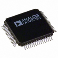
ADAV801ASTZ Analog Devices Inc, ADAV801ASTZ Datasheet - Page 58

ADAV801ASTZ
Manufacturer Part Number
ADAV801ASTZ
Description
IC CODEC AUDIO R-DVD 3.3V 64LQFP
Manufacturer
Analog Devices Inc
Type
Audio Codecr
Datasheet
1.ADAV801ASTZ-REEL.pdf
(60 pages)
Specifications of ADAV801ASTZ
Data Interface
Serial
Resolution (bits)
24 b
Number Of Adcs / Dacs
2 / 2
Sigma Delta
No
Dynamic Range, Adcs / Dacs (db) Typ
102 / 101
Voltage - Supply, Analog
3 V ~ 3.6 V
Voltage - Supply, Digital
3 V ~ 3.6 V
Operating Temperature
-40°C ~ 85°C
Mounting Type
Surface Mount
Package / Case
64-LQFP
Audio Codec Type
Stereo
No. Of Adcs
2
No. Of Dacs
2
No. Of Input Channels
2
No. Of Output Channels
2
Adc / Dac Resolution
24bit
Adcs / Dacs Signal To Noise Ratio
102dB
Single Supply Voltage (typ)
3.3V
Single Supply Voltage (min)
3V
Single Supply Voltage (max)
3.6V
Package Type
LQFP
Adc/dac Resolution
24b
Interface Type
Serial (SPI)
Mounting
Surface Mount
Number Of Adc's
2
Number Of Dac's
2
Operating Supply Voltage (max)
3.6V
Operating Supply Voltage (min)
3V
Operating Supply Voltage (typ)
3.3V
Operating Temperature (max)
85C
Operating Temperature (min)
-40C
Pin Count
64
Power Supply Type
Analog/Digital
Sample Rate
96KSPS
Screening Level
Industrial
Lead Free Status / RoHS Status
Lead free / RoHS Compliant
For Use With
EVAL-ADAV801EBZ - BOARD EVALUATION FOR ADAV801
Lead Free Status / Rohs Status
Compliant
Available stocks
Company
Part Number
Manufacturer
Quantity
Price
Company:
Part Number:
ADAV801ASTZ
Manufacturer:
ADI
Quantity:
455
Company:
Part Number:
ADAV801ASTZ
Manufacturer:
Analog Devices Inc
Quantity:
10 000
Part Number:
ADAV801ASTZ
Manufacturer:
ADI/亚德诺
Quantity:
20 000
Company:
Part Number:
ADAV801ASTZ-REEL
Manufacturer:
Analog Devices Inc
Quantity:
10 000
ADAV801
LAYOUT CONSIDERATIONS
Getting the best performance from the ADAV801 requires a
careful layout of the printed circuit board (PCB). Using separate
analog and digital ground planes is recommended, because
these give the currents a low resistance path back to the power
supplies. The ground planes should be connected in only one
place, usually under the ADAV801, to prevent ground loops.
The analog and digital supply pins should be decoupled to their
respective ground pins with a 10 μF to 47 μF tantalum capacitor
and a 0.1 μF ceramic capacitor. These capacitors should be
placed as close as possible to the supply pins.
ADC
The ADC uses a switch capacitor input stage and is, therefore,
particularly sensitive to digital noise. Sources of noise, such as
PLLs or clocks, should not be routed close to the ADC section.
The CAPxN and CAPxP pins form a charge reservoir for the
switched capacitor section of the ADC, so keeping these nodes
electrically quiet is a key factor in ensuring good performance.
The capacitors connected to these pins should be of good
quality, either NPO or COG, and should be placed as close as
possible to CAPxN and CAPxP.
DAC
The DAC requires an analog filter to filter out-of-band noise
from the analog output. A third-order Bessel filter is
recommended, although the filter to use depends on the
requirements of the application.
PLL
The PLL can be used to generate digital clocks, either for use
internally or to clock external circuitry. Because every clock is a
potential source of noise, care should be taken when using the
PLL. The ADAV801’s PLL outputs can be enabled or disabled,
as required. If the PLL clocks are not required by external
circuitry, it is recommended that the outputs be disabled. To
reduce cross-coupling between clocks, a digital ground trace
can be routed on either side of the PLL clock signal, if required.
Rev. A | Page 58 of 60
The PLL has its own power supply pins. To get the best
performance from the PLL and from the rest of the ADAV801,
it is recommended that a separate analog supply be used. Where
this is not possible, the user must decide whether to connect the
PLL supply to the analog (AVDD) or digital (DVDD) supply.
Connecting the PLL supply to AVDD gives the best jitter
performance, but can degrade the performance of the ADC and
DAC sections slightly due to the increased digital noise created
on the AVDD by the PLL. Connecting the PLL supply to DVDD
keeps digital noise away from the analog supply, but the jitter
specifications might be reduced depending on the quality of the
digital supply. Using the layout recommendations described in
this section helps to reduce these effects.
RESET AND POWER-DOWN CONSIDERATIONS
When the ADAV801 is held in reset by bringing the RESET
pin low, a number of circuit blocks remain powered up. For
example, the crystal oscillator circuit based around the XIN
and XOUT pins is still active, so that a stable clock source is
available when the ADAV801 is taken out of reset. In addition,
the VCO associated with the S/PDIF receiver is active so that
the receiver locks to the incoming S/PDIF stream in the shortest
possible time. Where power consumption is a concern, the
individual blocks of the ADAV801 can be powered down via
the control registers to gain significant power savings. Table 146
shows typical power savings when using the power-down bits
in the control registers.
Table 146. Typical Power Requirements
Operating
Mode
Normal
Reset low
Power-down
bits
AV
(mA)
50
30
12
DD
DV
(mA)
25
4
0.1
DD
ODV
(mA)
5
2.5
1.3
DD
DIR_V
(mA)
5
1
0.7
DD
Power
(mW)
280.5
123.75
46.53


