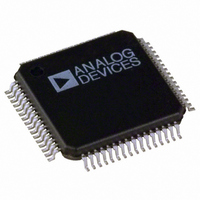
ADAV801ASTZ Analog Devices Inc, ADAV801ASTZ Datasheet - Page 18

ADAV801ASTZ
Manufacturer Part Number
ADAV801ASTZ
Description
IC CODEC AUDIO R-DVD 3.3V 64LQFP
Manufacturer
Analog Devices Inc
Type
Audio Codecr
Datasheet
1.ADAV801ASTZ-REEL.pdf
(60 pages)
Specifications of ADAV801ASTZ
Data Interface
Serial
Resolution (bits)
24 b
Number Of Adcs / Dacs
2 / 2
Sigma Delta
No
Dynamic Range, Adcs / Dacs (db) Typ
102 / 101
Voltage - Supply, Analog
3 V ~ 3.6 V
Voltage - Supply, Digital
3 V ~ 3.6 V
Operating Temperature
-40°C ~ 85°C
Mounting Type
Surface Mount
Package / Case
64-LQFP
Audio Codec Type
Stereo
No. Of Adcs
2
No. Of Dacs
2
No. Of Input Channels
2
No. Of Output Channels
2
Adc / Dac Resolution
24bit
Adcs / Dacs Signal To Noise Ratio
102dB
Single Supply Voltage (typ)
3.3V
Single Supply Voltage (min)
3V
Single Supply Voltage (max)
3.6V
Package Type
LQFP
Adc/dac Resolution
24b
Interface Type
Serial (SPI)
Mounting
Surface Mount
Number Of Adc's
2
Number Of Dac's
2
Operating Supply Voltage (max)
3.6V
Operating Supply Voltage (min)
3V
Operating Supply Voltage (typ)
3.3V
Operating Temperature (max)
85C
Operating Temperature (min)
-40C
Pin Count
64
Power Supply Type
Analog/Digital
Sample Rate
96KSPS
Screening Level
Industrial
Lead Free Status / RoHS Status
Lead free / RoHS Compliant
For Use With
EVAL-ADAV801EBZ - BOARD EVALUATION FOR ADAV801
Lead Free Status / Rohs Status
Compliant
Available stocks
Company
Part Number
Manufacturer
Quantity
Price
Company:
Part Number:
ADAV801ASTZ
Manufacturer:
ADI
Quantity:
455
Company:
Part Number:
ADAV801ASTZ
Manufacturer:
Analog Devices Inc
Quantity:
10 000
Part Number:
ADAV801ASTZ
Manufacturer:
ADI/亚德诺
Quantity:
20 000
Company:
Part Number:
ADAV801ASTZ-REEL
Manufacturer:
Analog Devices Inc
Quantity:
10 000
ADAV801
DAC SECTION
The ADAV801 has two DAC channels arranged as a stereo pair
with single-ended analog outputs. Each channel has its own
independently programmable attenuator, adjustable in 128 steps
of 0.375 dB per step. The DAC can receive data from the
playback or auxiliary input ports, the SRC, the ADC, or the
DIR. Each analog output pin sits at a dc level of VREF, and
swings 1.0 V rms for a 0 dB digital input signal. A single op amp
third-order external low-pass filter is recommended to remove
high frequency noise present on the output pins. Note that the
use of op amps with low slew rate or low bandwidth can cause
high frequency noise and tones to fold down into the audio
band. Care should be taken in selecting these components.
The FILTD and VREF pins should be bypassed by external
capacitors to AGND. The FILTD pin is used to reduce the noise
of the internal DAC bias circuitry, thereby reducing the DAC
output noise. The voltage at the VREF pin can be used to bias
external op amps used to filter the output signals. For
applications in which the VREF is required to drive external
op amps, which might draw more than 50 μA or have dynamic
load changes, extra buffering should be used to preserve the
quality of the ADAV801 reference.
The digital input data source for the DAC can be selected from
a number of available sources by programming the appropriate
bits in the datapath control register. Figure 27 shows how the
digital data source and the MCLK source for the DAC are
selected. Each DAC has an independent volume register giving
256 steps of control, with each step giving approximately
0.375 dB of attenuation. Note that the DACs are muted by
default to prevent unwanted pops, clicks, and other noises
from appearing on the outputs while the ADAV801 is being
configured. Each DAC also has a peak-level register that records
the peak value of the digital audio data. Reading the register
clears the peak.
ANALOG
OUTPUT
DAC
DAC
MODULATOR
MULTIBIT
Σ-Δ
Figure 28. DAC Block Diagram
TO ZERO FLAG PINS
Rev. A | Page 18 of 60
INTERPOLATOR
TO CONTROL
REGISTERS
Selecting a Sample Rate
Correct operation of the DAC is dependent upon the data rate
provided to the DAC, the master clock applied to the DAC, and
the selected interpolation rate. By default, the DAC assumes
that the MCLK rate is 256 times the sample rate, which requires
an 8× oversampling rate. This combination is suitable for
sample rates of up to 48 kHz.
For a 96 kHz data rate that has a 24.576 MHz MCLK (256 × f
associated with it, the DAC MCLK divider should be set to
divide the MCLK by 2. This prevents the DAC engine from
running too fast. To compensate for the reduced MCLK rate,
the interpolator should be selected to operate in 4 × (DAC
MCLK = 128 × f
different sample rates.
VOLUME/MUTE
ZERO DETECT
DETECTOR
CONTROL
PEAK
Figure 27. Clock and Datapath Control on the DAC
S
DIVIDER
). Similar combinations can be selected for
MCLK
MCLK
DAC
DAC
INPUT
DAC
FROM DAC
DATAPATH
MULTIPLEXER
REG 0x65
BITS[3:2]
REG 0x76
BITS[7:5]
REG 0x63
BITS[5:3]
ADC
AUXILIARY IN
PLAYBACK
DIR
S
)


