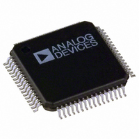
ADAV801ASTZ Analog Devices Inc, ADAV801ASTZ Datasheet - Page 55

ADAV801ASTZ
Manufacturer Part Number
ADAV801ASTZ
Description
IC CODEC AUDIO R-DVD 3.3V 64LQFP
Manufacturer
Analog Devices Inc
Type
Audio Codecr
Datasheet
1.ADAV801ASTZ-REEL.pdf
(60 pages)
Specifications of ADAV801ASTZ
Data Interface
Serial
Resolution (bits)
24 b
Number Of Adcs / Dacs
2 / 2
Sigma Delta
No
Dynamic Range, Adcs / Dacs (db) Typ
102 / 101
Voltage - Supply, Analog
3 V ~ 3.6 V
Voltage - Supply, Digital
3 V ~ 3.6 V
Operating Temperature
-40°C ~ 85°C
Mounting Type
Surface Mount
Package / Case
64-LQFP
Audio Codec Type
Stereo
No. Of Adcs
2
No. Of Dacs
2
No. Of Input Channels
2
No. Of Output Channels
2
Adc / Dac Resolution
24bit
Adcs / Dacs Signal To Noise Ratio
102dB
Single Supply Voltage (typ)
3.3V
Single Supply Voltage (min)
3V
Single Supply Voltage (max)
3.6V
Package Type
LQFP
Adc/dac Resolution
24b
Interface Type
Serial (SPI)
Mounting
Surface Mount
Number Of Adc's
2
Number Of Dac's
2
Operating Supply Voltage (max)
3.6V
Operating Supply Voltage (min)
3V
Operating Supply Voltage (typ)
3.3V
Operating Temperature (max)
85C
Operating Temperature (min)
-40C
Pin Count
64
Power Supply Type
Analog/Digital
Sample Rate
96KSPS
Screening Level
Industrial
Lead Free Status / RoHS Status
Lead free / RoHS Compliant
For Use With
EVAL-ADAV801EBZ - BOARD EVALUATION FOR ADAV801
Lead Free Status / Rohs Status
Compliant
Available stocks
Company
Part Number
Manufacturer
Quantity
Price
Company:
Part Number:
ADAV801ASTZ
Manufacturer:
ADI
Quantity:
455
Company:
Part Number:
ADAV801ASTZ
Manufacturer:
Analog Devices Inc
Quantity:
10 000
Part Number:
ADAV801ASTZ
Manufacturer:
ADI/亚德诺
Quantity:
20 000
Company:
Part Number:
ADAV801ASTZ-REEL
Manufacturer:
Analog Devices Inc
Quantity:
10 000
PLL Clock Source Register—Address 1111000 (0x78)
Table 136. PLL Clock Source Register Bit Map
7
PLL2_Source
Table 137. PLL Clock Source Register Bit Descriptions
Bit Name
PLL2_Source
PLL1_Source
PLL Output Enable—Address 1111010 (0x7A)
Table 138. PLL Output Enable Register Bit Map
7
Reserved
Table 139. PLL Output Enable Register Bit Descriptions
Bit Name
DIRINPD
DIRIN_PIN
SYSCLK1
SYSCLK2
SYSCLK3
6
PLL1_Source
6
Reserved
Description
Selects the clock source for PLL2.
Selects the clock source for PLL1.
Description
This bit powers down the S/PDIF receiver.
This bit determines the input levels of the DIRIN pin.
Enables the SYSCLK1 output.
Enables the SYSCLK2 output.
Enables the SYSCLK3 output.
0 = XIN.
1 = MCLKI.
0 = XIN.
1 = MCLKI
0 = Normal.
1 = Power-down.
0 = DIRIN accepts input signals down to 200 mV according to AES3 requirements.
1 = DIRIN accepts input signals as defined in the Specifications section.
0 = Enabled.
1 = Disabled.
0 = Enabled.
1 = Disabled.
0 = Enabled.
1 = Disabled.
5
Reserved
5
DIRINPD
4
Reserved
4
DIRIN_PIN
Rev. A | Page 55 of 60
3
Reserved
3
Reserved
2
Reserved
2
SYSCLK1
1
Reserved
1
SYSCLK2
0
Reserved
0
SYSCLK3
ADAV801


