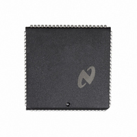
DP8344BV National Semiconductor, DP8344BV Datasheet - Page 59

DP8344BV
Manufacturer Part Number
DP8344BV
Description
IC BIPHASE COMM PROCESSR 84-PLCC
Manufacturer
National Semiconductor
Datasheet
1.DP8344BV.pdf
(184 pages)
Specifications of DP8344BV
Processor Type
8-Bit RISC
Speed
20MHz
Voltage
4.5 ~ 5.5V
Mounting Type
Surface Mount
Package / Case
84-PLCC
Operating Supply Voltage (typ)
5V
Operating Supply Voltage (max)
5.5V
Operating Supply Voltage (min)
4.5V
Mounting
Surface Mount
Operating Temperature (max)
70C
Operating Temperature (min)
0C
Operating Temperature Classification
Commercial
Lead Free Status / RoHS Status
Contains lead / RoHS non-compliant
Features
-
Lead Free Status / Rohs Status
Not Compliant
Other names
*DP8344BV
Available stocks
Company
Part Number
Manufacturer
Quantity
Price
Company:
Part Number:
DP8344BV
Manufacturer:
NSC
Quantity:
5 510
Part Number:
DP8344BV
Manufacturer:
NS/国半
Quantity:
20 000
3 0 Transceiver
3 2 5 Line Interface
3 2 5 1 3270 Line Interface
In the 3270 environment data is transmitted between a con-
trol unit and a device via a single coax cable or twisted pair
cable The coax type is RG62AU with a maximum length of
1 5 kilometers The twisted pair cable has become more
prevalent to reduce cabling and routing costs Typically a
24 AWG unshielded twisted pair is used to achieve the cost
reduction goals The length of the twisted pair cable is a
minimum of 100 feet to a maximum of 900 feet The 3270
protocol utilizes a transformer to isolate the peripheral from
the cabling system
An effective line interface design must be able to accept
either coax or twisted pair cabling and compensate for
noise jitter and reflections in the cabling system There
must be an adequate amount of jitter tolerance to offset the
effects of filtering and noise Some filtering is needed to
reduce ambient noise caused by surrounding hardware
Such filtering must not introduce transients that the receiver
comparator translates into data jitter
An effective driver design should also attempt to compen-
sate for the filtering effects of the cable Higher data fre-
quencies become attenuated more than lower frequency
signals as cable length is increased yielding greater dispari-
ty in the amplitudes of these signals This effect generates
greater jitter at the receiver The 3270 signal format allows
for a high voltage (predistorted) magnitude and a low volt-
age (nondistorted) magnitude within each data bit time In-
creasing the predistorted-to-nondistorted signal level ratio
counteracts the filtering phenomenon because the lower
frequency signals contain less predistortion than do higher
frequency signals Thus the amplitude of the higher fre-
quency signals is ‘‘boosted’’ more than the lower frequency
signals Unfortunately a low signal level is more susceptible
to reflection-induced errors at short cable length Proper im-
pedance matching and slower edge rates must be utilized to
eliminate as much reflection as possible at these lengths
Additionally shielded or balanced operation must be ade-
quately supported Shielded operation implies the use of
coax cable where balanced implies the use of twisted pair
cable Proper termination should be employed and a termi-
nation slightly greater than the characteristic impedance of
theline may actually provide more desirable waveforms
A
B
C
To coax twisted pair front end
To line driver circuitry
To BCP comparator
Includes board capacitance
Legend
(Continued)
FIGURE 3-12 BCP Receiver Design
59
3-12 An offset of approximately 17 mV separates the com-
than a perfectly matched termination Board layout should
make the comparator lines as short as possible Lines
should be placed closely together to avoid the introduction
of differential noise These lines should not pass near
‘‘noisy’’ lines A ground plane should isolate all ‘‘noisy’’
lines
BCP Design
The line interface design for the receiver is shown in Figure
parator inputs making the receiver more immune to ambi-
ent noise present on the circuit board A 2 1 1 (arranged as
a 3 1) transformer increases any voltage sensitivity lost by
introducing the offset A bandpass filter is employed to re-
duce edge rate to the comparator and eliminate ambient
noise The bandwidth (30 kHz to 30 MHz) was chosen to
provide sufficient attenuation for noise while producing mini-
mum data jitter
The driver design Figure 3-13 incorporates a National
Semiconductor DS3487 and a resistor network to generate
the proper signal levels The predistorted-to-nondistorted
ratio was chosen to be about 3 to 1 The coax twisted pair
front end Figure 3-14 includes an ADC brand connector to
switch between coax and twisted pair cable The coax inter-
face has the shield capacitively coupled to ground The
510
about 95
and possesses an input impedance of about 100
termination is somewhat higher than the characteristic im-
pedance (about 96 ) of twisted pair Terminations of this
type produce reflections that do not tend to generate mid-bit
errors Such terminations have the benefit of creating a larg-
er voltage at the receiver over longer cable lengths For a
more detailed explanation of the 3270 line interface see
Application Note ‘‘A Combined Coax Twisted Pair 3270
Line Interface for the DP8344 Biphase Communications
Processor’’
3 2 5 2 5250 Line Interface
The 5250 environment utilizes twinax in a multi-drop config-
uration where eight devices can be ‘‘daisy-chained’’ over a
total distance of 5 000 feet and eleven splices (each physi-
cal device is considered a splice) Twinax connectors are
bulky and expensive but are very sturdy Twinaxial cable is
a shielded twisted pair that is nearly
resistor and the filter loading produce a termination of
The twisted pair interface balances both lines
of an inch thick
TL F 9336 – G1
This


