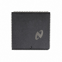
DP8344BV National Semiconductor, DP8344BV Datasheet - Page 176

DP8344BV
Manufacturer Part Number
DP8344BV
Description
IC BIPHASE COMM PROCESSR 84-PLCC
Manufacturer
National Semiconductor
Datasheet
1.DP8344BV.pdf
(184 pages)
Specifications of DP8344BV
Processor Type
8-Bit RISC
Speed
20MHz
Voltage
4.5 ~ 5.5V
Mounting Type
Surface Mount
Package / Case
84-PLCC
Operating Supply Voltage (typ)
5V
Operating Supply Voltage (max)
5.5V
Operating Supply Voltage (min)
4.5V
Mounting
Surface Mount
Operating Temperature (max)
70C
Operating Temperature (min)
0C
Operating Temperature Classification
Commercial
Lead Free Status / RoHS Status
Contains lead / RoHS non-compliant
Features
-
Lead Free Status / Rohs Status
Not Compliant
Other names
*DP8344BV
Available stocks
Company
Part Number
Manufacturer
Quantity
Price
Company:
Part Number:
DP8344BV
Manufacturer:
NSC
Quantity:
5 510
Part Number:
DP8344BV
Manufacturer:
NS/国半
Quantity:
20 000
Transceiver TCS1 0 Transceiver Clock
Control
(Continued)
Transmitter ATA
Control
Receiver
Control
6 0 Reference Section
6 2 3 Bit Definition Tables (Continued)
6 2 3 2 Transceiver (Continued)
Table includes control and status bits only It does not include definitions of bit fields provided for the formatting (de-formatting)
data frames For further information see the Transceiver section
TRES
AT7 –3
FB7 –0
OWP
TF10 –8 Transmit FIFO
TIN
AT7 –0
RF10 –8 Receive FIFO
RIN
RLQ
RPEN
SEC
Bit
Select
Transceiver RESet
Advance Transmitter TCR 4
Active
Auxiliary
Transceiver control
Fill Bit select
Odd Word Parity
Transmitter INvert
Auxiliary
Transceiver control
Receiver INvert
Receive Line
Quiesce
RePeat ENable
Select Error Codes
Name
(Continued)
DCR 6 5
TMR 7
ATR 7–3
FBR 7–0 XXXX XXXX The value in this register contains the 1’s complement of the
TCR 3
TCR 2– 0
TMR 3
ATR 7– 0 XXXX XXXX In 5250 modes AT2–0 contains the station address In 8-bit
TSR 2–0
TMR 4
TCR 7
TMR 5
TCR 6
Location Reset State
XXXXX
XXX
000
10
0
0
0
0
0
1
0
0
176
Selects transceiver clock TCLK source
OCLK is the frequency of the on-chip oscillator or the
externally applied clock on input X1 X-TCLK is the external
transceiver clock input
Resets transceiver when high Transceiver can also be reset
by RESET without affecting TRES
When high TX-ACT is advanced one half bit time so that the
transmitter can generate 5 5 line quiesce pulses
In 5250 modes Controls the time TX-ACT is held after the last
fill bit
number of additional 5250 fill bits selected
Controls transmitter word parity
transmit FIFO on moves to RTR
When high the transmitter serial data outputs are inverted
modes AT7 –0 contains the station address
Reflects the state of the most significant 3 bits in the top
location of the receive FIFO
When high the receiver serial data is inverted
Selects number of line quiesce bits the receiver requires
before it will indicate receipt of a valid start sequence
When high the receiver can be active at the same time as the
transmitter
When high ECR is switched into RTR location
OWP
TF10– 8 and RTF7– 0 are pushed onto the
RLQ Number of Line Quiesce Pulses
0 0 0 0 0
0 0 0 0 1
0 0 0 1 0
1 1 1 1 1
0
1
AT7– 3
OWP
TCS1 0
0
1
0 0
0 1
1 0
1 1
TX-ACT Hold Time ( s)
Function
(If TCLK
Word Parity
Even
Odd
OCLK
OCLK 2
OCLK 4
X-TCLK
TCLK
2
3
15 5
0 5
0
1
e
8 MHz)


