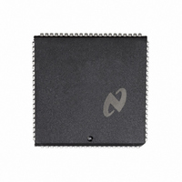
DP8344BV National Semiconductor, DP8344BV Datasheet - Page 55

DP8344BV
Manufacturer Part Number
DP8344BV
Description
IC BIPHASE COMM PROCESSR 84-PLCC
Manufacturer
National Semiconductor
Datasheet
1.DP8344BV.pdf
(184 pages)
Specifications of DP8344BV
Processor Type
8-Bit RISC
Speed
20MHz
Voltage
4.5 ~ 5.5V
Mounting Type
Surface Mount
Package / Case
84-PLCC
Operating Supply Voltage (typ)
5V
Operating Supply Voltage (max)
5.5V
Operating Supply Voltage (min)
4.5V
Mounting
Surface Mount
Operating Temperature (max)
70C
Operating Temperature (min)
0C
Operating Temperature Classification
Commercial
Lead Free Status / RoHS Status
Contains lead / RoHS non-compliant
Features
-
Lead Free Status / Rohs Status
Not Compliant
Other names
*DP8344BV
Available stocks
Company
Part Number
Manufacturer
Quantity
Price
Company:
Part Number:
DP8344BV
Manufacturer:
NSC
Quantity:
5 510
Part Number:
DP8344BV
Manufacturer:
NS/国半
Quantity:
20 000
3 0 Transceiver
3 2 3 Transceiver Interrupts
The transceiver has access to 3 CPU interrupt vectors one
each for the transmitter and receiver and a third the Line
Turn-Around interrupt providing a fast turn around capability
between receiver and transmitter The receiver interrupt is
the CPU’s highest priority interrupt (excluding NMI) fol-
lowed by the transmitter and Line Turn-Around interrupts
respectively The three interrupt vector addresses and a full
description of the interrupts are given in Table 3-2
The receiver interrupt is user-selectable from 4 possible
sources (only 3 used at present) by specifying a 2-bit field
the Receiver Interrupt Select bits RIS1-0 in the Interrupt
Control Register ICR
3-3
The RFF
is full (or an error is detected) If the number of frames in a
received message is not exactly divisible by 3 one or two
words could be left in the FIFO at the end of the message
since the CPU would receive no indication of the presence
of that data it is recommended that this interrupt be used
together with the line turn-around interrupt whose service
routine can include a test for whether any data is present in
the receive FIFO
Receiver
Transmitter
Line Turn-Around
All receiver interrupts can be cleared by asserting TRES
The interrupt vector is obtained by concatenating
IBR with the vector address as shown
RFF
DAV
Not Used
RA
Interrupt
Interrupt
a
a
a
RE
RE
RE interrupt occurs only when the receive FIFO
Vector Address
A full description is given in Table
RIS1 0
(Continued)
0 0
0 1
1 0
1 1
000100
001000
001100
by reading from ECR
Set when RFF or RE asserted If activated by RFF indicating that the
receive FIFO is full interrupt is cleared by reading from RTR If activated by
from ECR
Set when DAV or RE asserted If activated by DAV
data is present in the receive FIFO interrupt is cleared by reading from RTR If
activated by RE indicating that an error has been detected interrupt is cleared
Reserved for future product enhancement
Set when RA asserted indicating the receipt of a valid start sequence cleared
by reading ECR or RTR
RE indicating that an error has been detected interrupt is cleared by reading
TABLE 3-2 Transceiver Interrupts
User selectable from 4 possible sources see Table 3-3
Set when TFE asserted indicating that the transmit FIFO is empty cleared by
writing to RTR Note TRES causes TFE to be asserted
Set when a valid end sequence is detected cleared by writing to RTR writing
a one to LTA or asserting TRES In 5250 modes interrupt is set when the
last fill bit has been received and no further input transitions are detected Will
not be set in 5250 or 8-bit non-promiscuous modes unless an address match
was received
TABLE 3-3 Receiver Interrupts
15
IBR
55
For additional information concerning interrupts refer to
Sections 2 1 1 3 Interrupt Control Registers and 2 2 3 In-
terrupts
3 2 4 Protocol Modes
3270 3299 Modes
As shown in Table 3-1 the transceiver can operate in 4
different 3270 3299 modes to accommodate applications
of the BCP in different positions in the network The 3270
mode is designed for use in a device or a controller which is
not in a multiplexed environment For a multiplexed network
the 3299 multiplexer and controller modes are designed for
each end of the controller to multiplexer connection the
3299 repeater mode being used for an in-line repeater situ-
ated between controller and multiplexer
For information on how parallel data loaded into the trans-
mit FIFO and unloaded from the receive FIFO maps into the
serial bit positions see Figure 3-9
To transmit a frame
the correct control information after which the data byte
can be written to RTR
word is loaded into the transmit FIFO where it propagates
through to the last location to be loaded into the encoder
and formatted for transmission
When formatting a 3270 frame
the transmitter is required to format a data frame or a com-
mand frame If TCR 2
8
0 0
Description
Description
5
vector address
TCR 3– 0
is low the transmitter logic calcu-
The resulting composite 12-bit
0
TCR 2
interrupt
must first be set up with
vector
indicating that valid
controls whether


