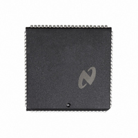
DP8344BV National Semiconductor, DP8344BV Datasheet - Page 154

DP8344BV
Manufacturer Part Number
DP8344BV
Description
IC BIPHASE COMM PROCESSR 84-PLCC
Manufacturer
National Semiconductor
Datasheet
1.DP8344BV.pdf
(184 pages)
Specifications of DP8344BV
Processor Type
8-Bit RISC
Speed
20MHz
Voltage
4.5 ~ 5.5V
Mounting Type
Surface Mount
Package / Case
84-PLCC
Operating Supply Voltage (typ)
5V
Operating Supply Voltage (max)
5.5V
Operating Supply Voltage (min)
4.5V
Mounting
Surface Mount
Operating Temperature (max)
70C
Operating Temperature (min)
0C
Operating Temperature Classification
Commercial
Lead Free Status / RoHS Status
Contains lead / RoHS non-compliant
Features
-
Lead Free Status / Rohs Status
Not Compliant
Other names
*DP8344BV
Available stocks
Company
Part Number
Manufacturer
Quantity
Price
Company:
Part Number:
DP8344BV
Manufacturer:
NSC
Quantity:
5 510
Part Number:
DP8344BV
Manufacturer:
NS/国半
Quantity:
20 000
6 0 Reference Section
SUBA Subtract with Accumulator
Syntax
SUBA
SUBA
Affected Flags
N Z C V
Description
Subtracts the active accumulator from the source register
Rs and places the result into the destination specified The
destination may be either a register Rd or data memory via
an index register mode mlr Negative numbers are repre-
sented using the two’s complement format Note that regis-
ter bank selection determines which accumulator is active
Example
In the first example the value 4 is placed into the currently
active accumulator that accumulator is subtracted from the
contents of register 20 and then the result is placed into
register 21
In the second example the alternate accumulator of regis-
ter bank B is selected and then subtracted from register 20
The result is placed into the data memory pointed to by the
index register IZ and then the value of IZ is incremented by
one
Instruction Format
SUBA Rs Rd
T-states
SUBA Rs Rd
SUBA Rs mlr
Bus Timing
SUBA Rs Rd
SUBA Rs mlr
Operation
SUBA Rs Rd
Rs
SUBA Rs mlr
Rs
1
15
SUBA Rs mlr
MOVE 4 A
SUBA
EXX
SUBA
b
b
1
accumulator
accumulator
Opcode
1
Rs Rd
Rs mlr
R20 R21
0 1
R20 IZ
0
1
a
0
Figure 6-1
Figure 6-7
2
3
Rd
data memory
register register
register indexed
9
and increment data pointer
Place constant into accum
R20
Select alt accumulator
R20
b
b
Rd
accum
accum
(Continued)
4
R21
data mem
TL F 9336– 16
Rs
0
154
Figure 6-1
TRAP Software Interrupt
Syntax
TRAP v
Affected Flags
None
Description
Pushes the Program Counter the Global Interrupt Enable bit
tions onto the internal Address Stack then unconditionally
transfers control to the instruction at the memory address
created by concatenating the contents of the Interrupt Base
Register IBR to the value of v extended with zeros to 8
bits If the value of g is equal to ‘‘1’’ then the Global Inter-
rupt Enable bit GIE will be cleared If the g operand is
omitted then g
points to one of 64 Interrupt Table entries (range 0 to 63)
Since some of the Interrupt Table entries are used by the
hardware interrupts the TRAP instruction can simulate
hardware interrupts The following table lists the hardware
interrupts and their associated vector numbers
Example
Simulate the Transmitter FIFO Empty interrupt
Instruction Format
T-states
2
Bus Timing
Operation
PC
if g
Create PC address by concatonating the IBR register to
the vector number v as shown below
GIE the ALU flags and the current register bank selec-
1
15
TRAP
then clear GIE
e
1
Address Stack
GIE
1
0
g
NMI
RFF DA RA
TFE
LTA
BIRQ
TO
Interrupt
0
Hardware Interrupt Vector Table
8 1
Opcode
ALU flags
1
e
1
0 is assumed The vector number v
TFE interrupt simulation
1
1
register bank selections
28
12
16
20
1
v
4
8
g
6
5
(011100)
(000100)
(001000)
(001100)
(010000)
(010100)
(Binary)
v
TL F 9336– 17
0


