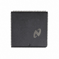
DP8344BV National Semiconductor, DP8344BV Datasheet - Page 20

DP8344BV
Manufacturer Part Number
DP8344BV
Description
IC BIPHASE COMM PROCESSR 84-PLCC
Manufacturer
National Semiconductor
Datasheet
1.DP8344BV.pdf
(184 pages)
Specifications of DP8344BV
Processor Type
8-Bit RISC
Speed
20MHz
Voltage
4.5 ~ 5.5V
Mounting Type
Surface Mount
Package / Case
84-PLCC
Operating Supply Voltage (typ)
5V
Operating Supply Voltage (max)
5.5V
Operating Supply Voltage (min)
4.5V
Mounting
Surface Mount
Operating Temperature (max)
70C
Operating Temperature (min)
0C
Operating Temperature Classification
Commercial
Lead Free Status / RoHS Status
Contains lead / RoHS non-compliant
Features
-
Lead Free Status / Rohs Status
Not Compliant
Other names
*DP8344BV
Available stocks
Company
Part Number
Manufacturer
Quantity
Price
Company:
Part Number:
DP8344BV
Manufacturer:
NSC
Quantity:
5 510
Part Number:
DP8344BV
Manufacturer:
NS/国半
Quantity:
20 000
2 0 CPU Description
2 1 3 Instruction Set
The followng paragraphs introduce the BCP’s architecture
by discussing addressing modes and briefly discussing the
Instruction Set For detailed explanations and examples of
each instruction refer to the Instruction Set Reference Sec-
tion
2 1 3 1 Harvard Architecture Implications
The BCP utilizes a true Harvard Architecture where the in-
struction and data memory are organized into two indepen-
dent memory banks each with their own address and data
buses Both the Instruction Address Bus and the Instruction
Bus are 16 bits wide with the Instruction Address Bus ad-
dressing memory by words (A word of memory is 16 bits
long i e 1 word
one word long The exceptions are two words long contain-
ing a word of instruction followed by a word of immediate
data The combination of word sized instructions and a word
based instruction address bus eliminates the typical instruc-
tion alignment problems faced by many CPU’s
The Data Address Bus is 16 bits wide (with the low order 8
bits multiplexed on the Data Bus) and the Data Bus is 8 bits
wide (i e one byte wide) The Data Address Bus addresses
memory by bytes Most of the BCP’s instructions operate on
byte-sized operands
Note that although both instruction addresses and data ad-
dresses are 16 bits long these addresses are for two differ-
ent buses and therefore have two different numerical
meanings (i e byte address or word address ) Each in-
struction determines whether the meaning of a 16-bit ad-
dress is that of an instruction word address or a data byte
address Little confusion exists though because only the
program flow instructions interpret 16-bit addresses as in-
struction addresses
Notation
e
Rs
Rd
Rsd
rs
rd
rsd
2 bytes ) Most of the instructions are
(Continued)
Source Register
Destination Register
Register is both a Source
Limited Source Register
Limited Destination Register
Limited Register is both a Source
Notation
TABLE 2-2 Immediate Addressing Mode Notations
TABLE 2-1 Register Addressing Mode Notations
n
nn
Type of Register Operand
Type of Immediate Operand
Immediate Number
Absolute Number
20
Destination
2 1 3 2 Addressing Modes
An addressing mode is the mechanism by which an instruc-
tion accesses its operand(s) The BCP’s architecture sup-
ports five basic addressing modes register immediate in-
dexed immediate-relative and register-relative The first
two allow instructions to execute the fastest because they
require no memory access beyond instruction fetch The
remaining three addressing modes point to data or instruc-
tion memory Typical of a RISC processor most of the in-
structions only support the first three addressing modes
with one of the operands always limited to the register ad-
dressing mode
Register Addressing Modes
There are two terminologies for the register addressing
modes Register and Limited Register Instructions that al-
low Register operands can access all the registers in the
CPU Note that only 32 of the 44 CPU registers are available
at any given point in time because the lower 12 register
locations (R0 – R11) access one of two switchable register
banks each (See Section 2 1 1 1 Banked Registers for
more information on the CPU register banks ) Instructions
that allow the Limited Register operands can access just
the first 28 registers of the CPU Again note that only 16 of
these 28 registers are available at any given point in time
Table 2-1 shows the notations used for the Register and
Limited Register operands Some instructions also imply the
use of certain registers for example the accumulators This
is noted in the discussions of those instructions
Immediate Addressing Modes
The two types of the immediate addressing modes available
are Immediate numbers and Absolute numbers Immediate
numbers are 8 bits of data (one data byte) that code direct-
ly into the instruction word Immediate numbers may repre-
sent data data address displacements or relative instruc-
tion addresses Absolute numbers are 16-bit numbers They
code into the second word of two word instructions and they
represent absolute instruction addresses Table 2-2 shows
the notations used for both of these addressing modes
Destination
16 Bits
Size
8 Bits
Registers Allowed
R0– R31
R0– R31
R0– R31
R0– R15
R0– R15
R0 – R15


