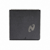
DP8344BV National Semiconductor, DP8344BV Datasheet - Page 25

DP8344BV
Manufacturer Part Number
DP8344BV
Description
IC BIPHASE COMM PROCESSR 84-PLCC
Manufacturer
National Semiconductor
Datasheet
1.DP8344BV.pdf
(184 pages)
Specifications of DP8344BV
Processor Type
8-Bit RISC
Speed
20MHz
Voltage
4.5 ~ 5.5V
Mounting Type
Surface Mount
Package / Case
84-PLCC
Operating Supply Voltage (typ)
5V
Operating Supply Voltage (max)
5.5V
Operating Supply Voltage (min)
4.5V
Mounting
Surface Mount
Operating Temperature (max)
70C
Operating Temperature (min)
0C
Operating Temperature Classification
Commercial
Lead Free Status / RoHS Status
Contains lead / RoHS non-compliant
Features
-
Lead Free Status / Rohs Status
Not Compliant
Other names
*DP8344BV
Available stocks
Company
Part Number
Manufacturer
Quantity
Price
Company:
Part Number:
DP8344BV
Manufacturer:
NSC
Quantity:
5 510
Part Number:
DP8344BV
Manufacturer:
NS/国半
Quantity:
20 000
JRMK
2 0 CPU Description
The BCP also has a specialized relative jump instruction
called relative Jump with Rotate and Mask on source regis-
ter JRMK This instruction facilitates the decoding of regis-
ter fields often involved in communications processing
JRMK does this by rotating and masking a copy of its regis-
ter operand to form a signed program counter displacement
which usually points into a jump table Table 2-15 shows the
syntax and operation of the JRMK instruction
JRMK’s masking (setting to zero) the least significant bit of
the displacement allows the construction of a jump table
using either one or two word instructions for instance a
table of JMP and or LJMP instructions respectively The
example in Figure 2-6 demonstrates the JRMK instruction
decoding the address frame of the 3299 Terminal Multiplex-
Note PC
Note PC
CALL
LCALL
Example Code
JRMK
LJMP
LJMP
LJMP
Syntax
GIE
(a) Copy RTR into JRMK’s displacement register
(b) Rotate displacement register 1 bit to the right
(c) AND result with ‘‘00001110’’ binary mask
(d) Sign extend resulting displacement and add
(e) Execute the instruction pointed to by the PC
Syntax
e
e
e
concatenation operator combines operands together forming one long operand
e
Program Counter contents initially points to instruction following jump
Program Counter contents initially points to instruction following call
Rs b m
it to the program counter (PC)
If the bits A2 A1 A0 equal ‘‘0 0 1’’ binary then
(i e PC
which in this example is
n
nn
a
RTR 1 4
ADDR 0
ADDR 1
ADDR 7
Global Interrupt Enable bit
LJMP ADDR 1
2 is added to the Program Counter
a
2
(a) Rotate a copy of register ‘‘Rs’’ ‘‘b’’ bits to the right
(b) Mask the most significant ‘‘m’’ bits and the least
(c) PC
PC
PC
PC
nn
Instruction Execution
decode terminal address
jump to device handler
jump to device handler
jump to device handler
significant bit of the above result
a
PC)
n (sign extended)
a
GIE
GIE
PC
(Continued)
resulting displacement (sign extended)
ALU flags
ALU flags
TABLE 2-16 Unconditional Call Instructions
Instruction Operation
FIGURE 2-6 JRMK Instruction Example
Instruction Operation
TABLE 2-15 JRMK Instruction
reg bank selection
reg bank selection
PC
0
1
7
25
er protocol which is located in the Receive Transmit Regis-
ter
The BCP has two unconditional call instructions CALL
which supports relative instruction addressing and LCALL
(Long CALL) which supports absolute instruction address-
ing These instructions push the following information onto
the CPU’s internal Address Stack the address of the next
instruction the status of the Global Interrupt Enable flag
the status of which register banks are currently active Table
2-16 lists the two unconditional call instructions Note that
the Address Stack is only twelve positions deep therefore
the BCP allows twelve levels of nested subroutine invoca-
tions (this includes both interrupts and calls)
GIE the status of the ALU flags Z
RTR 4–2
x
y
0
0
Address Stack
Address Stack
JRMK Displacement Register Contents
PC
x
x
0
0
x
x
0
0
Displacement
b
128
A2
0
0
x
Range
b
Operand
128
a
Range
0 64k
126
A1
A2
A2
0
a
127
A0
A1
A1
0
C
Addressing Mode
Addressing Mode
N and V and
A0
A0
y
1
Register
Immediate
Absolute
0
0
y
y


