ADSP-3PARCBF548M01 Analog Devices Inc, ADSP-3PARCBF548M01 Datasheet - Page 79
ADSP-3PARCBF548M01
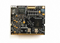
Manufacturer Part Number
ADSP-3PARCBF548M01
Description
MODULE BOARD BF548
Manufacturer
Analog Devices Inc
Series
Blackfin®r
Specifications of ADSP-3PARCBF548M01
Module/board Type
Processor Module
For Use With/related Products
ADSP-BF548
Lead Free Status / RoHS Status
Lead free / RoHS Compliant


ATAPI Ultra DMA Data-In Transfer Timing
Table 60
ultra DMA data-in data transfer timing.
Table 60. ATAPI Ultra DMA Data-In Transfer Timing
1
2
ATAPI Parameter
t
t
t
t
t
t
t
t
t
t
t
ATAPI Timing Register Setting should be programmed with a value that guarantees parameter compliance with the ATA ANSI specification for ATA device mode of operation.
This timing equation can be used to calculate both the minimum and maximum t
DS
DH
CVS
CVH
LI
MLI
AZ
ZAH
ENV
RP
ACK
2
and
Data setup time at host
Data hold time at host
CRC word valid setup time at host
CRC word valid hold time at host
Limited interlock time
Interlock time with minimum
Maximum time allowed for output drivers to
release
Minimum delay time required for output
ATAPI_DMACK to ATAPI_DIOR/DIOW
ATAPI_DMACK to ATAPI_DIOR/DIOW
Setup and hold times for ATAPI_DMACK
Figure 52
through
ADSP-BF542/ADSP-BF544/ADSP-BF547/ADSP-BF548/ADSP-BF549
Figure 55
describe the ATAPI
Rev. C | Page 79 of 100 | February 2010
ATAPI_ULTRA_TIM_x Timing
Register Setting
N/A
N/A
TDVS
TACK
N/A
TZAH, TCVS
N/A
TZAH
TENV
TRP
TACK
ENV
.
1
Timing Equation
T
T
TDVS × t
TACK × t
2 × t
(TZAH + TCVS) × t
0
2 × t
(TENV × t
TRP × t
TACK × t
SK3
SK3
+ t
+ t
BD
SCLK
+ 2 × t
SUDU
HDU
SCLK
+ TZAH × t
SCLK
SCLK
SCLK
SCLK
– (t
– (t
– (t
– (t
) +/- (t
SCLK
SK1
SK1
SK1
SK1
+ t
+ t
SCLK
+ t
+ t
+ t
SCLK
SK1
SK2
OD
SK2
– (4 × t
SK2
SK2
+ t
+ t
+ t
)
)
)
SK2
SCLK
SK4
)
BD
)
+ 4 × t
SCLK
+ 2 × t
OD
)
Related parts for ADSP-3PARCBF548M01
Image
Part Number
Description
Manufacturer
Datasheet
Request
R

Part Number:
Description:
±1.7g Dual-Axis IMEMS Accelerometer Evaluation Board
Manufacturer:
Analog Devices Inc
Datasheet:

Part Number:
Description:
Inertial Sensor Evaluation System
Manufacturer:
Analog Devices Inc
Datasheet:
Part Number:
Description:
Manufacturer:
Analog Devices Inc
Datasheet:
Part Number:
Description:
Manufacturer:
Analog Devices Inc
Datasheet:
Part Number:
Description:
Manufacturer:
Analog Devices Inc
Datasheet:
Part Number:
Description:
Manufacturer:
Analog Devices Inc
Datasheet:
Part Number:
Description:
Manufacturer:
Analog Devices Inc
Datasheet:
Part Number:
Description:
Manufacturer:
Analog Devices Inc
Datasheet:
Part Number:
Description:
Manufacturer:
Analog Devices Inc
Datasheet:
Part Number:
Description:
Manufacturer:
Analog Devices Inc
Datasheet:
Part Number:
Description:
Manufacturer:
Analog Devices Inc
Datasheet:
Part Number:
Description:
Manufacturer:
Analog Devices Inc
Datasheet:
Part Number:
Description:
Manufacturer:
Analog Devices Inc
Datasheet: