ADSP-3PARCBF548M01 Analog Devices Inc, ADSP-3PARCBF548M01 Datasheet - Page 22
ADSP-3PARCBF548M01
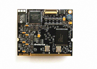
Manufacturer Part Number
ADSP-3PARCBF548M01
Description
MODULE BOARD BF548
Manufacturer
Analog Devices Inc
Series
Blackfin®r
Specifications of ADSP-3PARCBF548M01
Module/board Type
Processor Module
For Use With/related Products
ADSP-BF548
Lead Free Status / RoHS Status
Lead free / RoHS Compliant


ADSP-BF542/ADSP-BF544/ADSP-BF547/ADSP-BF548/ADSP-BF549
By default, the boot kernel will always issue five address cycles;
therefore, if a large page device requires only four cycles, the
device must be capable of ignoring the additional address cycle.
16-bit NAND flash memory devices must only support the issu-
ing of command and address cycles via the lower eight bits of
the data bus. Devices that use the full 16-bit bus for command
and address cycles are not supported.
• Boot from OTP memory (BMODE = 0xB)—This provides
• Boot from 16-bit host DMA (BMODE = 0xE)—In this
• Boot from 8-bit host DMA (BMODE = 0xF)—In this
a standalone booting method. The boot stream is loaded
from on-chip OTP memory. By default, the boot stream is
expected to start from OTP page 0x40 and can occupy all
public OTP memory up to page 0xDF (2560 bytes). Since
the start page is programmable, the maximum size of the
boot stream can be extended to 3072 bytes.
mode, the host DMA port is configured in 16-bit acknowl-
edge mode with little endian data format. Unlike other
modes, the host is responsible for interpreting the boot
stream. It writes data blocks individually into the host
DMA port. Before configuring the DMA settings for each
block, the host may either poll the ALLOW_CONFIG bit in
HOST_STATUS or wait to be interrupted by the HWAIT
signal. When using HWAIT, the host must still check
ALLOW_CONFIG at least once before beginning to con-
figure the host DMA port. After completing the
configuration, the host is required to poll the READY bit in
HOST_STATUS before beginning to transfer data. When
the host sends an HIRQ control command, the boot kernel
issues a CALL instruction to address 0xFFA0 0000. It is the
host’s responsibility to ensure valid code has been placed at
this address. The routine at address 0xFFA0 0000 can be a
simple initialization routine to configure internal
resources, such as the SDRAM controller, which then
returns using an RTS instruction. The routine may also be
the final application, which will never return to the boot
kernel.
mode, the host DMA port is configured in 8-bit interrupt
mode with little endian data format. Unlike other modes,
the host is responsible for interpreting the boot stream. It
writes data blocks individually to the host DMA port.
Before configuring the DMA settings for each block, the
host may either poll the ALLOW_CONFIG bit in
HOST_STATUS or wait to be interrupted by the HWAIT
signal. When using HWAIT, the host must still check
ALLOW_CONFIG at least once before beginning to con-
figure the host DMA port. The host will receive an
interrupt from the HOST_ACK signal every time it is
allowed to send the next FIFO depth’s worth (sixteen 32-bit
words) of information. When the host sends an HIRQ con-
trol command, the boot kernel issues a CALL instruction to
address 0xFFA0 0000. It is the host's responsibility to
ensure valid code has been placed at this address. The rou-
tine at address 0xFFA0 0000 can be a simple initialization
routine to configure internal resources, such as the
Rev. C | Page 22 of 100 | February 2010
For each of the boot modes, a 16-byte header is first read from
an external memory device. The header specifies the number of
bytes to be transferred and the memory destination address.
Multiple memory blocks may be loaded by any boot sequence.
Once all blocks are loaded, program execution commences from
the address stored in the EVT1 register.
Prior to booting, the pre-boot routine interrogates the OTP
memory. Individual boot modes can be customized or disabled
based on OTP programming. External hardware, especially
booting hosts, may monitor the HWAIT signal to determine
when the pre-boot has finished and the boot kernel starts the
boot process. However, the HWAIT signal does not toggle in
NAND boot mode. By programming OTP memory, the user
can instruct the preboot routine to also customize the PLL, volt-
age regulator, DDR controller, and/or asynchronous memory
interface controller.
The boot kernel differentiates between a regular hardware reset
and a wakeup-from-hibernate event to speed up booting in the
later case. Bits 6-4 in the system reset configuration (SYSCR)
register can be used to bypass the pre-boot routine and/or boot
kernel in case of a software reset. They can also be used to simu-
late a wakeup-from-hibernate boot in the software reset case.
The boot process can be further customized by “initialization
code.” This is a piece of code that is loaded and executed prior to
the regular application boot. Typically, this is used to configure
the DDR controller or to speed up booting by managing PLL,
clock frequencies, wait states, and/or serial bit rates.
The boot ROM also features C-callable function entries that can
be called by the user application at run time. This enables sec-
ond-stage boot or booting management schemes to be
implemented with ease.
INSTRUCTION SET DESCRIPTION
The Blackfin processor family assembly language instruction set
employs an algebraic syntax designed for ease of coding and
readability. The instructions have been specifically tuned to pro-
vide a flexible, densely encoded instruction set that compiles to
a very small final memory size. The instruction set also provides
fully featured multifunction instructions that allow the pro-
grammer to use many of the processor core resources in a single
instruction. Coupled with many features more often seen on
microcontrollers, this instruction set is very efficient when com-
piling C and C++ source code. In addition, the architecture
supports both user (algorithm/application code) and supervisor
(O/S kernel, device drivers, debuggers, ISRs) modes of opera-
tion, allowing multiple levels of access to core processor
resources.
SDRAM controller, which then returns using an RTS
instruction. The routine may also be the final application,
which will never return to the boot kernel.
Related parts for ADSP-3PARCBF548M01
Image
Part Number
Description
Manufacturer
Datasheet
Request
R

Part Number:
Description:
±1.7g Dual-Axis IMEMS Accelerometer Evaluation Board
Manufacturer:
Analog Devices Inc
Datasheet:

Part Number:
Description:
Inertial Sensor Evaluation System
Manufacturer:
Analog Devices Inc
Datasheet:
Part Number:
Description:
Manufacturer:
Analog Devices Inc
Datasheet:
Part Number:
Description:
Manufacturer:
Analog Devices Inc
Datasheet:
Part Number:
Description:
Manufacturer:
Analog Devices Inc
Datasheet:
Part Number:
Description:
Manufacturer:
Analog Devices Inc
Datasheet:
Part Number:
Description:
Manufacturer:
Analog Devices Inc
Datasheet:
Part Number:
Description:
Manufacturer:
Analog Devices Inc
Datasheet:
Part Number:
Description:
Manufacturer:
Analog Devices Inc
Datasheet:
Part Number:
Description:
Manufacturer:
Analog Devices Inc
Datasheet:
Part Number:
Description:
Manufacturer:
Analog Devices Inc
Datasheet:
Part Number:
Description:
Manufacturer:
Analog Devices Inc
Datasheet:
Part Number:
Description:
Manufacturer:
Analog Devices Inc
Datasheet: