ADSP-3PARCBF548M01 Analog Devices Inc, ADSP-3PARCBF548M01 Datasheet - Page 48
ADSP-3PARCBF548M01
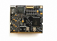
Manufacturer Part Number
ADSP-3PARCBF548M01
Description
MODULE BOARD BF548
Manufacturer
Analog Devices Inc
Series
Blackfin®r
Specifications of ADSP-3PARCBF548M01
Module/board Type
Processor Module
For Use With/related Products
ADSP-BF548
Lead Free Status / RoHS Status
Lead free / RoHS Compliant


ADSP-BF542/ADSP-BF544/ADSP-BF547/ADSP-BF548/ADSP-BF549
DDR SDRAM/Mobile DDR SDRAM Clock and Control Cycle Timing
Table 32
SDRAM clock and control cycle timing.
Table 32. DDR SDRAM/Mobile DDR SDRAM Clock and Control Cycle Timing
1
2
3
Parameter
Switching Characteristics
t
t
t
t
t
t
The t
Address pins include DA0-12 and DBA0-1.
Control pins include DCS0-1, DCLKE, DRAS, DCAS, and DWE.
CK
CH
CL
AS
AH
OPW
1
2,3
2,3
2,3
CK
specification does not account for the effects of jitter.
and
Figure 17
DCK0-1 Period
DCK0-1 High Pulse Width
DCK0-1 Low Pulse Width
Address and Control Output SETUP Time Relative to CK
Address and Control Output HOLD Time Relative to CK
Address and Control Output Pulse Width
describe DDR SDRAM/mobile DDR
ADDRESS
CONTROL
DCK0-1
Figure 17. DDR SDRAM /Mobile DDR SDRAM Clock and Control Cycle Timing
t
AS
NOTE: CONTROL = DCS0-1, DCLKE, DRAS, DCAS, AND DWE.
t
OPW
ADDRESS = DA0-12 AND DBA0-1.
Rev. C | Page 48 of 100 | February 2010
t
AH
t
CK
DDR SDRAM
Min
7.50
1.00
1.00
2.20
0.45
0.45
t
CH
Max
0.55
0.55
t
CL
Mobile DDR SDRAM
Min
7.50
0.45
1.00
1.00
2.30
0.45
Max
8.33
0.55
0.55
Unit
ns
t
t
ns
ns
ns
CK
CK
Related parts for ADSP-3PARCBF548M01
Image
Part Number
Description
Manufacturer
Datasheet
Request
R

Part Number:
Description:
±1.7g Dual-Axis IMEMS Accelerometer Evaluation Board
Manufacturer:
Analog Devices Inc
Datasheet:

Part Number:
Description:
Inertial Sensor Evaluation System
Manufacturer:
Analog Devices Inc
Datasheet:
Part Number:
Description:
Manufacturer:
Analog Devices Inc
Datasheet:
Part Number:
Description:
Manufacturer:
Analog Devices Inc
Datasheet:
Part Number:
Description:
Manufacturer:
Analog Devices Inc
Datasheet:
Part Number:
Description:
Manufacturer:
Analog Devices Inc
Datasheet:
Part Number:
Description:
Manufacturer:
Analog Devices Inc
Datasheet:
Part Number:
Description:
Manufacturer:
Analog Devices Inc
Datasheet:
Part Number:
Description:
Manufacturer:
Analog Devices Inc
Datasheet:
Part Number:
Description:
Manufacturer:
Analog Devices Inc
Datasheet:
Part Number:
Description:
Manufacturer:
Analog Devices Inc
Datasheet:
Part Number:
Description:
Manufacturer:
Analog Devices Inc
Datasheet:
Part Number:
Description:
Manufacturer:
Analog Devices Inc
Datasheet: