ADSP-3PARCBF548M01 Analog Devices Inc, ADSP-3PARCBF548M01 Datasheet - Page 14
ADSP-3PARCBF548M01
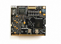
Manufacturer Part Number
ADSP-3PARCBF548M01
Description
MODULE BOARD BF548
Manufacturer
Analog Devices Inc
Series
Blackfin®r
Specifications of ADSP-3PARCBF548M01
Module/board Type
Processor Module
For Use With/related Products
ADSP-BF548
Lead Free Status / RoHS Status
Lead free / RoHS Compliant


ADSP-BF542/ADSP-BF544/ADSP-BF547/ADSP-BF548/ADSP-BF549
The ADSP-BF54x Blackfin processors’ CAN controllers offer
the following features:
The electrical characteristics of each network connection are
very demanding, so the CAN interface is typically divided into
two parts: a controller and a transceiver. This allows a single
controller to support different drivers and CAN networks. The
ADSP-BF54x Blackfin processors’ CAN module represents only
the controller part of the interface. The controller interface sup-
ports connection to 3.3 V high speed, fault-tolerant, single-wire
transceivers.
An additional crystal is not required to supply the CAN clock, as
the CAN clock is derived from the processor system clock
(SCLK) through a programmable divider.
TWI CONTROLLER INTERFACE
The ADSP-BF54x Blackfin processors include up to two 2-wire
interface (TWI) modules for providing a simple exchange
method of control data between multiple devices. The modules
are compatible with the widely used I
modules offer the capabilities of simultaneous master and slave
operation and support for both 7-bit addressing and multime-
dia data arbitration. Each TWI interface uses two pins for
transferring clock (SCLx) and data (SDAx), and supports the
protocol at speeds up to 400K bits/sec. The TWI interface pins
are compatible with 5 V logic levels.
Additionally, the ADSP-BF54x Blackfin processors’ TWI mod-
ules are fully compatible with serial camera control bus (SCCB)
functionality for easier control of various CMOS camera sensor
devices.
PORTS
Because of their rich set of peripherals, the ADSP-BF54x
Blackfin processors group the many peripheral signals to ten
ports—referred to as Port A to Port J. Most ports contain 16
pins, though some have fewer. Many of the associated pins are
shared by multiple signals. The ports function as multiplexer
controls. Every port has its own set of memory-mapped regis-
ters to control port muxing and GPIO functionality.
• 32 mailboxes (8 receive only, 8 transmit only, 16 config-
• Dedicated acceptance masks for each mailbox.
• Additional data filtering on first two bytes.
• Support for both the standard (11-bit) and extended (29-
• Support for remote frames.
• Active or passive network support.
• CAN wakeup from hibernation mode (lowest static power
• Interrupts, including: TX complete, RX complete, error
urable for receive or transmit).
bit) identifier (ID) message formats.
consumption mode).
and global.
2
C bus standard. The TWI
Rev. C | Page 14 of 100 | February 2010
General-Purpose I/O (GPIO)
Every pin in Port A to Port J can function as a GPIO pin, result-
ing in a GPIO pin count up to 154. While it is unlikely that all
GPIO pins will be used in an application, as all pins have multi-
ple functions, the richness of GPIO functionality guarantees
unrestrictive pin usage. Every pin that is not used by any func-
tion can be configured in GPIO mode on an individual basis.
After reset, all pins are in GPIO mode by default. Since neither
GPIO output nor input drivers are active by default, unused
pins can be left unconnected. GPIO data and direction control
registers provide flexible write-one-to-set and write-one-to-
clear mechanisms so that independent software threads do not
need to protect against each other because of expensive read-
modify-write operations when accessing the same port.
Pin Interrupts
Every port pin on ADSP-BF54x Blackfin processors can request
interrupts in either an edge-sensitive or a level-sensitive manner
with programmable polarity. Interrupt functionality is decou-
pled from GPIO operation. Four system-level interrupt
channels (PINT0, PINT1, PINT2 and PINT3) are reserved for
this purpose. Each of these interrupt channels can manage up to
32 interrupt pins. The assignment from pin to interrupt is not
performed on a pin-by-pin basis. Rather, groups of eight pins
(half ports) can be flexibly assigned to interrupt channels.
Every pin interrupt channel features a special set of 32-bit mem-
ory-mapped registers that enables half-port assignment and
interrupt management. This not only includes masking, identi-
fication, and clearing of requests, it also enables access to the
respective pin states and use of the interrupt latches regardless
of whether the interrupt is masked or not. Most control registers
feature multiple MMR address entries to write-one-to-set or
write-one-to-clear them individually.
PIXEL COMPOSITOR (PIXC)
The pixel compositor (PIXC) provides image overlays with
transparent-color support, alpha blending, and color space con-
version capabilities for output to TFT LCDs and NTSC/PAL
video encoders. It provides all of the control to allow two data
streams from two separate data buffers to be combined,
blended, and converted into appropriate forms for both LCD
panels and digital video outputs. The main image buffer pro-
vides the basic background image, which is presented in the
data stream. The overlay image buffer allows the user to add
multiple foreground text, graphics, or video objects on top of
the main image or video data stream.
ENHANCED PARALLEL PERIPHERAL INTERFACE
(EPPI)
The ADSP-BF54x Blackfin processors provide up to three
enhanced parallel peripheral interfaces (EPPIs), supporting data
widths up to 24 bits. The EPPI supports direct connection to
TFT LCD panels, parallel analog-to-digital and digital-to-ana-
log converters, video encoders and decoders, image sensor
modules and other general-purpose peripherals.
Related parts for ADSP-3PARCBF548M01
Image
Part Number
Description
Manufacturer
Datasheet
Request
R

Part Number:
Description:
±1.7g Dual-Axis IMEMS Accelerometer Evaluation Board
Manufacturer:
Analog Devices Inc
Datasheet:

Part Number:
Description:
Inertial Sensor Evaluation System
Manufacturer:
Analog Devices Inc
Datasheet:
Part Number:
Description:
Manufacturer:
Analog Devices Inc
Datasheet:
Part Number:
Description:
Manufacturer:
Analog Devices Inc
Datasheet:
Part Number:
Description:
Manufacturer:
Analog Devices Inc
Datasheet:
Part Number:
Description:
Manufacturer:
Analog Devices Inc
Datasheet:
Part Number:
Description:
Manufacturer:
Analog Devices Inc
Datasheet:
Part Number:
Description:
Manufacturer:
Analog Devices Inc
Datasheet:
Part Number:
Description:
Manufacturer:
Analog Devices Inc
Datasheet:
Part Number:
Description:
Manufacturer:
Analog Devices Inc
Datasheet:
Part Number:
Description:
Manufacturer:
Analog Devices Inc
Datasheet:
Part Number:
Description:
Manufacturer:
Analog Devices Inc
Datasheet:
Part Number:
Description:
Manufacturer:
Analog Devices Inc
Datasheet: