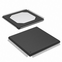
XC3S100E-4TQG144I Xilinx Inc, XC3S100E-4TQG144I Datasheet - Page 98

XC3S100E-4TQG144I
Manufacturer Part Number
XC3S100E-4TQG144I
Description
IC FPGA SPARTAN-3E 100K 144-TQFP
Manufacturer
Xilinx Inc
Series
Spartan™-3Er
Datasheet
1.XC3S100E-4TQG144I.pdf
(193 pages)
Specifications of XC3S100E-4TQG144I
Package / Case
144-TQFP, 144-VQFP
Mounting Type
Surface Mount
Voltage - Supply
1.1 V ~ 3.465 V
Operating Temperature
-40°C ~ 100°C
Number Of I /o
108
Number Of Logic Elements/cells
*
Number Of Gates
*
Lead Free Status / RoHS Status
Lead free / RoHS Compliant
Available stocks
Company
Part Number
Manufacturer
Quantity
Price
Company:
Part Number:
XC3S100E-4TQG144I
Manufacturer:
XILINX/21
Quantity:
163
Company:
Part Number:
XC3S100E-4TQG144I
Manufacturer:
Xilinx Inc
Quantity:
10 000
Part Number:
XC3S100E-4TQG144I
Manufacturer:
XILINX/赛灵思
Quantity:
20 000
- Current page: 98 of 193
- Download datasheet (2Mb)
The FPGA signals when the memory-clearing phase is
complete by releasing the open-drain INIT_B pin, allowing
the pin to go High via the external pull-up resistor to
VCCO_2.
Loading Configuration Data
Configuration data is then written to the FPGA’s internal
memory. The FPGA holds the Global Set/Reset (GSR) sig-
nal active throughout configuration, holding all FPGA
flip-flops in a reset state. The FPGA signals when the entire
configuration process completes be releasing the DONE
pin, allowing it to go High.
The FPGA configuration sequence can also be initiated by
asserting the PROG_B. Once release, the FPGA begins
clearing its internal configuration memory, and progresses
through the remainder of the configuration process.
DS312-2 (v1.1) March 21, 2005
Advance Product Specification
R
Start-Up Clock
Start-Up Clock
Figure 66: Default Start-Up Sequence
Phase
DONE
Phase
DONE
GWE
GWE
GTS
GTS
www.xilinx.com
DONE High
0
0
1
1
Default Cycles
Sync-to-DONE
Start-Up
At the end of configuration, the Global Set/Reset (GSR) sig-
nal is pulsed, placing all flip-flops in a known state. After
configuration completes, the FPGA switches over to the
user application loaded into the FPGA. The sequence and
timing of how the FPGA switches over is programmable as
is the clock source controlling the sequence.
The default start-up sequence appears in
the Global Three-State signal (GTS) is released one clock
cycle after DONE goes High. This sequence allows the
DONE signal to enable or disable any external logic used
during configuration before the user application in the FPGA
starts driving output signals. One clock cycle later, the Glo-
bal Write Enable (GWE) signal is released. This allows sig-
nals to propagate within the FPGA before any clocked
storage elements such as flip-flops and block ROM are
enabled.
2
2
3
3
4
4
5
5
DS312-2_60_022305
6 7
6 7
Functional Description
Figure
66, where
91
Related parts for XC3S100E-4TQG144I
Image
Part Number
Description
Manufacturer
Datasheet
Request
R

Part Number:
Description:
IC SPARTAN-3E FPGA 100K 144-TQFP
Manufacturer:
Xilinx Inc
Datasheet:

Part Number:
Description:
FIELD PROGRAMMER
Manufacturer:
Xilinx Inc
Datasheet:

Part Number:
Description:
FPGA Spartan®-3E Family 100K Gates 2160 Cells 572MHz 90nm (CMOS) Technology 1.2V 100-Pin VTQFP
Manufacturer:
Xilinx Inc
Datasheet:

Part Number:
Description:
FPGA Spartan®-3E Family 100K Gates 2160 Cells 572MHz 90nm (CMOS) Technology 1.2V 144-Pin TQFP
Manufacturer:
Xilinx Inc
Datasheet:

Part Number:
Description:
FPGA Spartan®-3E Family 100K Gates 2160 Cells 657MHz 90nm (CMOS) Technology 1.2V 144-Pin TQFP
Manufacturer:
Xilinx Inc
Datasheet:

Part Number:
Description:
Spartan-3E FPGA Family
Manufacturer:
XILINX [Xilinx, Inc]
Datasheet:

Part Number:
Description:
Spartan-3E FPGA Family: Complete Data Sheet
Manufacturer:
XILINX [Xilinx, Inc]
Datasheet:

Part Number:
Description:
IC FPGA SPARTAN-3E 100K 100-VQFP
Manufacturer:
Xilinx Inc
Datasheet:

Part Number:
Description:
IC FPGA SPARTAN-3E 100K 132CSBGA
Manufacturer:
Xilinx Inc
Datasheet:

Part Number:
Description:
IC FPGA SPARTAN-3E 100K 132CSBGA
Manufacturer:
Xilinx Inc
Datasheet:

Part Number:
Description:
IC FPGA SPARTAN-3E 100K 144-TQFP
Manufacturer:
Xilinx Inc
Datasheet:

Part Number:
Description:
IC FPGA SPARTAN 3E 100VQFP
Manufacturer:
Xilinx Inc
Datasheet:

Part Number:
Description:
IC FPGA SPARTAN 3E 144TQFP
Manufacturer:
Xilinx Inc
Datasheet:

Part Number:
Description:
FPGA Spartan®-3E Family 100K Gates 2160 Cells 572MHz 90nm (CMOS) Technology 1.2V 132-Pin CSBGA
Manufacturer:
Xilinx Inc
Datasheet:

Part Number:
Description:
IC CPLD .8K 36MCELL 44-VQFP
Manufacturer:
Xilinx Inc
Datasheet:


