XC3S100E-4TQG144I Xilinx Inc, XC3S100E-4TQG144I Datasheet - Page 10
XC3S100E-4TQG144I
Manufacturer Part Number
XC3S100E-4TQG144I
Description
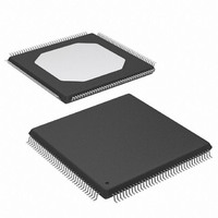
IC FPGA SPARTAN-3E 100K 144-TQFP
Manufacturer
Xilinx Inc
Series
Spartan™-3Er
Datasheet
1.XC3S100E-4TQG144I.pdf
(193 pages)
Specifications of XC3S100E-4TQG144I
Package / Case
144-TQFP, 144-VQFP
Mounting Type
Surface Mount
Voltage - Supply
1.1 V ~ 3.465 V
Operating Temperature
-40°C ~ 100°C
Number Of I /o
108
Number Of Logic Elements/cells
*
Number Of Gates
*
Lead Free Status / RoHS Status
Lead free / RoHS Compliant
Available stocks
Company
Part Number
Manufacturer
Quantity
Price
Company:

Part Number:
XC3S100E-4TQG144I
Manufacturer:
XILINX/21
Quantity:
163
Company:
Part Number:
XC3S100E-4TQG144I
Manufacturer:
Xilinx Inc
Quantity:
10 000
Part Number:
XC3S100E-4TQG144I
Manufacturer:
XILINX/赛灵思
Quantity:
20 000


Input Delay Functions
Each IOB has a programmable delay block that can delay
the input signal from 0 to nominally 4000 ps. In
signal is first delayed by either 0 or 2000 ps (nominal) and is
then applied to an 8 tap delay line. This delay line has a
nominal value of 250 ps per tap. All 8 taps are available via
a multiplexer for use as an asynchronous input directly into
the FPGA fabric. In this way, the delay is programmable
from 0 to 4000 ps in 250 ps steps. Four of the 8 taps are
also available via a multiplexer to the D inputs of the syn-
chronous storage elements. The delay inserted in the path
to the storage element can be varied from 0 to 4000 ps in
500 ps steps. The first, coarse delay element is common to
both asynchronous and synchronous paths, and must be
either used or not used for both paths.
DS312-2 (v1.1) March 21, 2005
Advance Product Specification
R
PAD
Figure 2: Input Delay Elements
Figure
2, the
www.xilinx.com
The delay values are set up in the silicon once at configura-
tion time—they are non-modifiable in device operation.
The primary use for the input delay element is as an ade-
quate delay to ensure that there is no hold time requirement
when using the input flip-flop(s) with a global clock. The
necessary value for this function is chosen by the Xilinx soft-
ware tools and depends on device size. If the design is
using a DCM in the clock path, then the delay element can
be safely set to zero in the user's design, and there is still no
hold time requirement.
Both asynchronous and synchronous values can be modi-
fied by the user, which is useful where extra delay is
required on clock or data inputs, for example, in interfaces to
various types of RAM.
See
for the delay elements.
Module 3
Asynchronous input (I)
Synchronous input (IQ1)
Synchronous input (IQ2)
of the Spartan-3E data sheet for exact values
D Q
D Q
DS312-2_18_022205
Functional Description
3
Related parts for XC3S100E-4TQG144I
Image
Part Number
Description
Manufacturer
Datasheet
Request
R

Part Number:
Description:
IC SPARTAN-3E FPGA 100K 144-TQFP
Manufacturer:
Xilinx Inc
Datasheet:

Part Number:
Description:
FIELD PROGRAMMER
Manufacturer:
Xilinx Inc
Datasheet:
Part Number:
Description:
FPGA Spartan®-3E Family 100K Gates 2160 Cells 572MHz 90nm (CMOS) Technology 1.2V 100-Pin VTQFP
Manufacturer:
Xilinx Inc
Datasheet:

Part Number:
Description:
FPGA Spartan®-3E Family 100K Gates 2160 Cells 572MHz 90nm (CMOS) Technology 1.2V 144-Pin TQFP
Manufacturer:
Xilinx Inc
Datasheet:
Part Number:
Description:
FPGA Spartan®-3E Family 100K Gates 2160 Cells 657MHz 90nm (CMOS) Technology 1.2V 144-Pin TQFP
Manufacturer:
Xilinx Inc
Datasheet:
Part Number:
Description:
Spartan-3E FPGA Family
Manufacturer:
XILINX [Xilinx, Inc]
Datasheet:
Part Number:
Description:
Spartan-3E FPGA Family: Complete Data Sheet
Manufacturer:
XILINX [Xilinx, Inc]
Datasheet:
Part Number:
Description:
IC FPGA SPARTAN-3E 100K 100-VQFP
Manufacturer:
Xilinx Inc
Datasheet:

Part Number:
Description:
IC FPGA SPARTAN-3E 100K 132CSBGA
Manufacturer:
Xilinx Inc
Datasheet:
Part Number:
Description:
IC FPGA SPARTAN-3E 100K 132CSBGA
Manufacturer:
Xilinx Inc
Datasheet:
Part Number:
Description:
IC FPGA SPARTAN-3E 100K 144-TQFP
Manufacturer:
Xilinx Inc
Datasheet:
Part Number:
Description:
IC FPGA SPARTAN 3E 100VQFP
Manufacturer:
Xilinx Inc
Datasheet:
Part Number:
Description:
IC FPGA SPARTAN 3E 144TQFP
Manufacturer:
Xilinx Inc
Datasheet:
Part Number:
Description:
FPGA Spartan®-3E Family 100K Gates 2160 Cells 572MHz 90nm (CMOS) Technology 1.2V 132-Pin CSBGA
Manufacturer:
Xilinx Inc
Datasheet:

Part Number:
Description:
IC CPLD .8K 36MCELL 44-VQFP
Manufacturer:
Xilinx Inc
Datasheet: