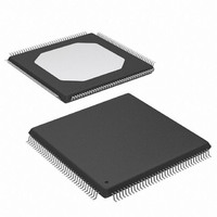
XC3S100E-4TQG144I Xilinx Inc, XC3S100E-4TQG144I Datasheet - Page 50

XC3S100E-4TQG144I
Manufacturer Part Number
XC3S100E-4TQG144I
Description
IC FPGA SPARTAN-3E 100K 144-TQFP
Manufacturer
Xilinx Inc
Series
Spartan™-3Er
Datasheet
1.XC3S100E-4TQG144I.pdf
(193 pages)
Specifications of XC3S100E-4TQG144I
Package / Case
144-TQFP, 144-VQFP
Mounting Type
Surface Mount
Voltage - Supply
1.1 V ~ 3.465 V
Operating Temperature
-40°C ~ 100°C
Number Of I /o
108
Number Of Logic Elements/cells
*
Number Of Gates
*
Lead Free Status / RoHS Status
Lead free / RoHS Compliant
Available stocks
Company
Part Number
Manufacturer
Quantity
Price
Company:
Part Number:
XC3S100E-4TQG144I
Manufacturer:
XILINX/21
Quantity:
163
Company:
Part Number:
XC3S100E-4TQG144I
Manufacturer:
Xilinx Inc
Quantity:
10 000
Part Number:
XC3S100E-4TQG144I
Manufacturer:
XILINX/赛灵思
Quantity:
20 000
ious values as described in
synthesis outputs are described in
Duty Cycle Correction of DLL Clock Outputs
The CLK2X
ordinarily exhibit a 50% duty cycle – even if the incoming
CLKIN signal has a different duty cycle. Fifty-percent duty
cycle means that the High and Low times of each clock
cycle are equal. The DUTY_CYCLE_CORRECTION
attribute determines whether or not duty cycle correction is
applied to the CLK0, CLK90, CLK180, and CLK270 outputs.
If DUTY_CYCLE_CORRECTION is set to TRUE, then the
duty cycle of these four outputs is corrected to 50%. If
DUTY_CYCLE_CORRECTION is set to FALSE, then these
outputs exhibit the same duty cycle as the CLKIN signal.
Figure 40
signals to those of the CLKIN signal.
The CLK2X output generates a 25% duty cycle clock at the
same frequency as the CLKIN signal until the DLL has
achieved lock.
The duty cycle of the CLKDV outputs may differ somewhat
from 50% (i.e., the signal is High for less than 50% of the
period) when the CLKDV_DIVIDE attribute is set to a
non-integer value and the DLL is operating in the High Fre-
quency mode.
Digital Frequency Synthesizer (DFS)
The DFS component generates clock signals the frequency
of which is a product of the clock frequency at the CLKIN
input and a ratio of two user-determined integers. Because
of the wide range of possible output frequencies such a ratio
permits, the DFS feature provides still further flexibility than
the DLL’s basic synthesis options as described in the pre-
ceding section. The DFS component’s two dedicated out-
puts, CLKFX and CLKFX180, are defined in
The signal at the CLKFX180 output is essentially an inver-
sion of the CLKFX signal. These two outputs always exhibit
a 50% duty cycle. This is true even when the CLKIN signal
does not. These DFS clock outputs are driven at the same
time as the DLL’s seven clock outputs.
The numerator of the ratio is the integer value assigned to
the attribute CLKFX_MULTIPLY and the denominator is the
integer value assigned to the attribute CLKFX_DIVIDE.
These attributes are described in
The output frequency (f
tion of the incoming clock frequency (f
f
Regarding the two attributes, it is possible to assign any
combination of integer values, provided that two conditions
are met:
1. The two values fall within their corresponding ranges,
DS312-2 (v1.1) March 21, 2005
Advance Product Specification
CLKFX
as specified in
= f
CLKIN
compares the characteristics of the DLL’s output
R
(1)
, CLK2X180, and CLKDV
*(CLKFX_MULTIPLY/CLKFX_DIVIDE) (3)
Table
CLKFX
27.
Table
) can be expressed as a func-
Table
26. The basic frequency
Table
CLKIN
27.
25.
(2)
) as follows:
Table
output signals
28.
www.xilinx.com
2. The f
For example, if CLKFX_MULTIPLY = 5 and CLKFX_DIVIDE
= 3, then the frequency of the output clock signal is 5/3 that
of the input clock signal.
DFS With or Without the DLL
The DFS component can be used with or without the DLL
component: Without the DLL, the DFS component multi-
plies or divides the CLKIN signal frequency according to the
respective CLKFX_MULTIPLY and CLKFX_DIVIDE values,
Phase:
Input Signal (30% Duty Cycle)
Output Signal - Duty Cycle is Always Corrected
Output Signal - Attribute Corrects Duty Cycle
CLK2X180
CLKDV
Figure 40: Characteristics of the DLL Clock Outputs
DUTY_CYCLE_CORRECTION = FALSE
CLK180
CLK270
DUTY_CYCLE_CORRECTION = TRUE
CLK180
CLK270
expression accords with the DCM’s operating frequency
specifications.
CLK2X
CLK90
CLK90
CLKIN
CLK0
CLK0
(1)
CLKFX
0
frequency calculated from the above
o
90
o
180
t
o
270
o
0
Functional Description
o
90
o
180
o
270
DS099-2_10_031303
o
0
o
43


