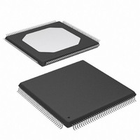
XC3S100E-4TQG144I Xilinx Inc, XC3S100E-4TQG144I Datasheet - Page 13

XC3S100E-4TQG144I
Manufacturer Part Number
XC3S100E-4TQG144I
Description
IC FPGA SPARTAN-3E 100K 144-TQFP
Manufacturer
Xilinx Inc
Series
Spartan™-3Er
Datasheet
1.XC3S100E-4TQG144I.pdf
(193 pages)
Specifications of XC3S100E-4TQG144I
Package / Case
144-TQFP, 144-VQFP
Mounting Type
Surface Mount
Voltage - Supply
1.1 V ~ 3.465 V
Operating Temperature
-40°C ~ 100°C
Number Of I /o
108
Number Of Logic Elements/cells
*
Number Of Gates
*
Lead Free Status / RoHS Status
Lead free / RoHS Compliant
Available stocks
Company
Part Number
Manufacturer
Quantity
Price
Company:
Part Number:
XC3S100E-4TQG144I
Manufacturer:
XILINX/21
Quantity:
163
Company:
Part Number:
XC3S100E-4TQG144I
Manufacturer:
Xilinx Inc
Quantity:
10 000
Part Number:
XC3S100E-4TQG144I
Manufacturer:
XILINX/赛灵思
Quantity:
20 000
Functional Description
Register Cascade Feature
In the Spartan-3E family, one of the IOBs in a differential
pair can cascade either its input or output storage elements
with those in the other IOB of the differential pair. This is
intended to make DDR operation at high speed much sim-
pler to implement. The new DDR connections that are avail-
able are shown in
available for routing between IOBs and are not accessible to
the FPGA fabric. Note that this feature is only available
when using differential I/O.
IDDR2
As a DDR input pair, the master IOB registers incoming
data on the rising edge of ICLK1 (= D1) and the rising edge
of ICLK2 (= D2), which is typically the same as the falling
edge of ICLK1. This data is then transferred into the FPGA
fabric. At some point, both signals must be brought into the
same clock domain, typically ICLK1. This can be difficult at
high frequencies because the available time is only one half
of a clock cycle assuming a 50% duty cycle. See
for a graphical illustration of this function.
In the Spartan-3E device, the signal D2 can be cascaded
into the storage element of the adjacent slave IOB. There it
is re-registered to ICLK1, and only then fed to the FPGA
fabric where it is now already in the same time domain as
D1. Here, the FPGA fabric uses only the clock ICLK1 to pro-
cess the received data. See
tion of this function.
6
ICLK1
ICLK2
PAD
D1
D2
Figure 4: Input DDR (without Cascade Feature)
d
PAD
d-1
d+1
d
d+2
d+1
Figure 1
d+3
d+2
Figure 5
d+4
(dashed lines), and are only
d+3
D
D
d+5
d+4
Q
Q
for a graphical illustra-
d+6
d+5
d+7
D1
To Fabric
D2
d+6
ICLK2
ICLK1
DS312-2_21_021105
d+8
Figure 4
d+7
www.xilinx.com
d+8
Figure 5: Input DDR Using Spartan-3E Cascade Feature
ODDR2
As a DDR output pair, the master IOB registers data coming
from the FPGA fabric on the rising edge of OCLK1 (= D1)
and the rising edge of OCLK2 (= D2), which is typically the
same as the falling edge of OCLK1. These two bits of data
are multiplexed by the DDR mux and forwarded to the out-
put pin. At some point in the FPGA fabric, the signal D2
must be brought into the clock domain OCLK2 from the
domain OCLK1. This can be difficult at high frequencies,
because the time available is only one half a clock cycle.
See
In the Spartan-3E device, the signal D2 can be cascaded
via the storage element of the adjacent slave IOB. Here, it is
registered by OCLK1 and then forwarded to the master IOB
where it is re-registered to OCLK2, selected as usual by the
DDR multiplexer, and then forwarded to the output pin. This
way the data for transmission can be processed using just
the clock OCLK1 in the FPGA fabric. See
graphical illustration of this function.
PAD
ICLK1
ICLK2
PAD
Figure 6
D1
D2
d
for a graphical illustration of this function.
d+1
D
D
d-1
d
Q
Q
d+2
IQ2
d+3
d+2
d+1
Advance Product Specification
d+4
IDDRIN2
DS312-2 (v1.1) March 21, 2005
d+5
d+4
d+3
D Q
d+6
d+7
Figure 7
d+5
d+6
To Fabric
DS312-2_22_030105
D1
D2
d+8
ICLK1
ICLK2
d+8
d+7
for a
R


