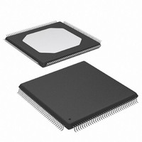
XC3S100E-4TQG144I Xilinx Inc, XC3S100E-4TQG144I Datasheet - Page 77

XC3S100E-4TQG144I
Manufacturer Part Number
XC3S100E-4TQG144I
Description
IC FPGA SPARTAN-3E 100K 144-TQFP
Manufacturer
Xilinx Inc
Series
Spartan™-3Er
Datasheet
1.XC3S100E-4TQG144I.pdf
(193 pages)
Specifications of XC3S100E-4TQG144I
Package / Case
144-TQFP, 144-VQFP
Mounting Type
Surface Mount
Voltage - Supply
1.1 V ~ 3.465 V
Operating Temperature
-40°C ~ 100°C
Number Of I /o
108
Number Of Logic Elements/cells
*
Number Of Gates
*
Lead Free Status / RoHS Status
Lead free / RoHS Compliant
Available stocks
Company
Part Number
Manufacturer
Quantity
Price
Company:
Part Number:
XC3S100E-4TQG144I
Manufacturer:
XILINX/21
Quantity:
163
Company:
Part Number:
XC3S100E-4TQG144I
Manufacturer:
Xilinx Inc
Quantity:
10 000
Part Number:
XC3S100E-4TQG144I
Manufacturer:
XILINX/赛灵思
Quantity:
20 000
- Current page: 77 of 193
- Download datasheet (2Mb)
Functional Description
Similarly, the SPI bus can be expanded to additional SPI
peripherals. Because SPI is a common industry-standard
interface, there are a variety of SPI-based peripherals avail-
able, including analog-to-digital (A/D) converters, digi-
tal-to-analog (D/A) converters, CAN controllers, and
temperature sensors.
The MOSI, DIN, and CCLK pins are common to all SPI
peripherals. Connect the select input on each additional SPI
peripheral to one of the FPGA user I/O pins. If HSWAP = 0
during configuration, the FPGA holds the select line High. If
HSWAP = 1, connect the select line to +3.3V via an external
4.7 kΩ pull-up resistor to avoid spurious read or write oper-
ations. After configuration, drive the select line Low to select
the desired SPI peripheral. Refer to the individual SPI
70
Spartan-3E FPGA
Figure 53: Using the SPI Flash Interface After Configuration
FPGA-based
SPI Master
User-I/O
CSO_B
CCLK
MOSI
To other SPI slave peripherals
DIN
www.xilinx.com
+3.3V
peripheral data sheet for specific interface and communica-
tion protocol requirements.
Daisy-Chaining
If the application requires multiple FPGAs with different con-
figurations, then configure the FPGAs using a daisy chain,
as
(M[2:0] = <0:0:1>) for the FPGA connected to the Platform
Flash PROM and Slave Serial mode (M[2:0] = <1:1:1>) for
all other FPGAs in the daisy-chain. After the master
FPGA—the FPGA on the left in the diagram—finishes load-
ing its configuration data from the SPI Flash PROM, the
master device uses its DOUT output pin to supply data to
the next device in the daisy-chain, on the falling CCLK edge.
shown
SPI Serial Flash PROM
SPI Peripherals
DATA_IN
DATA_OUT
CLOCK
DATA_IN
DATA_OUT
CLOCK
SELECT
SELECT
in
Figure
• A/D Converter
• D/A Converter
• CAN Controller
• Temperature Sensor
• Displays
• Temperature Sensor
• Microcontroller
• ASSP
54.
Configuration
Advance Product Specification
MicroBlaze
User Data
DS312-2 (v1.1) March 21, 2005
FPGA
Use
Code
DS312-2_47_022205
SPI
FFFFF
0
Flash
mode
R
Related parts for XC3S100E-4TQG144I
Image
Part Number
Description
Manufacturer
Datasheet
Request
R

Part Number:
Description:
IC SPARTAN-3E FPGA 100K 144-TQFP
Manufacturer:
Xilinx Inc
Datasheet:

Part Number:
Description:
FIELD PROGRAMMER
Manufacturer:
Xilinx Inc
Datasheet:

Part Number:
Description:
FPGA Spartan®-3E Family 100K Gates 2160 Cells 572MHz 90nm (CMOS) Technology 1.2V 100-Pin VTQFP
Manufacturer:
Xilinx Inc
Datasheet:

Part Number:
Description:
FPGA Spartan®-3E Family 100K Gates 2160 Cells 572MHz 90nm (CMOS) Technology 1.2V 144-Pin TQFP
Manufacturer:
Xilinx Inc
Datasheet:

Part Number:
Description:
FPGA Spartan®-3E Family 100K Gates 2160 Cells 657MHz 90nm (CMOS) Technology 1.2V 144-Pin TQFP
Manufacturer:
Xilinx Inc
Datasheet:

Part Number:
Description:
Spartan-3E FPGA Family
Manufacturer:
XILINX [Xilinx, Inc]
Datasheet:

Part Number:
Description:
Spartan-3E FPGA Family: Complete Data Sheet
Manufacturer:
XILINX [Xilinx, Inc]
Datasheet:

Part Number:
Description:
IC FPGA SPARTAN-3E 100K 100-VQFP
Manufacturer:
Xilinx Inc
Datasheet:

Part Number:
Description:
IC FPGA SPARTAN-3E 100K 132CSBGA
Manufacturer:
Xilinx Inc
Datasheet:

Part Number:
Description:
IC FPGA SPARTAN-3E 100K 132CSBGA
Manufacturer:
Xilinx Inc
Datasheet:

Part Number:
Description:
IC FPGA SPARTAN-3E 100K 144-TQFP
Manufacturer:
Xilinx Inc
Datasheet:

Part Number:
Description:
IC FPGA SPARTAN 3E 100VQFP
Manufacturer:
Xilinx Inc
Datasheet:

Part Number:
Description:
IC FPGA SPARTAN 3E 144TQFP
Manufacturer:
Xilinx Inc
Datasheet:

Part Number:
Description:
FPGA Spartan®-3E Family 100K Gates 2160 Cells 572MHz 90nm (CMOS) Technology 1.2V 132-Pin CSBGA
Manufacturer:
Xilinx Inc
Datasheet:

Part Number:
Description:
IC CPLD .8K 36MCELL 44-VQFP
Manufacturer:
Xilinx Inc
Datasheet:


