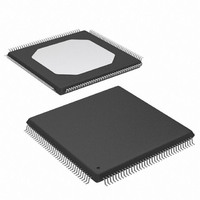
XC3S100E-4TQG144I Xilinx Inc, XC3S100E-4TQG144I Datasheet - Page 66

XC3S100E-4TQG144I
Manufacturer Part Number
XC3S100E-4TQG144I
Description
IC FPGA SPARTAN-3E 100K 144-TQFP
Manufacturer
Xilinx Inc
Series
Spartan™-3Er
Datasheet
1.XC3S100E-4TQG144I.pdf
(193 pages)
Specifications of XC3S100E-4TQG144I
Package / Case
144-TQFP, 144-VQFP
Mounting Type
Surface Mount
Voltage - Supply
1.1 V ~ 3.465 V
Operating Temperature
-40°C ~ 100°C
Number Of I /o
108
Number Of Logic Elements/cells
*
Number Of Gates
*
Lead Free Status / RoHS Status
Lead free / RoHS Compliant
Available stocks
Company
Part Number
Manufacturer
Quantity
Price
Company:
Part Number:
XC3S100E-4TQG144I
Manufacturer:
XILINX/21
Quantity:
163
Company:
Part Number:
XC3S100E-4TQG144I
Manufacturer:
Xilinx Inc
Quantity:
10 000
Part Number:
XC3S100E-4TQG144I
Manufacturer:
XILINX/赛灵思
Quantity:
20 000
- Current page: 66 of 193
- Download datasheet (2Mb)
Table 41
ous configuration pins during the configuration process. The
configuration interface is designed primarily for 2.5V opera-
tion when the VCCO_2 (and VCCO_1 in BPI mode) con-
nects to 2.5V.
The configuration pins also operate at other voltages by set-
ting VCCO_2 (and VCCO_1 in BPI mode) to either 3.3V or
1.8V. The change on the VCCO supply also changes the I/O
Table 41: Default I/O Standard Setting During Configuration (VCCO_2 = 2.5V)
Master Serial Mode
In Master Serial mode (M[2:0] = <0:0:0>), the Spartan-3E
FPGA configures itself from an attached Xilinx Platform
Flash PROM, as illustrated in
plies the CCLK output clock from its internal oscillator to the
DS312-2 (v1.1) March 21, 2005
Advance Product Specification
Recommend
open-drain
PROG_B
All, including CCLK
driver
TMS
TDO
TCK
shows the default I/O standard setting for the vari-
TDI
+2.5V
JTAG
R
Pin(s)
Serial Master
Mode
‘0’
‘0’
‘0’
P
Figure 48: Master Serial Mode using Platform Flash PROM
Figure
HSWAP
M2
M1
M0
TDI
TMS
TCK
PROG_B
48. The FPGA sup-
I/O Standard
Spartan-3E
LVCMOS25
VCCINT
+1.2V
GND
VCCAUX
VCCO_0
VCCO_2
INIT_B
DONE
DOUT
CCLK
TDO
DIN
www.xilinx.com
VCCO_0
+2.5V
V
drive characteristics. For example, with VCCO = 3.3V, the
output current when driving High, I
imately 12 to 16 mA, while the current when driving Low,
I
when driving High, I
6 to 8 mA. Again, the current when driving Low, I
8 mA.
attached Platform Flash PROM. In response, the Platform
Flash PROM supplies bit-serial data to the FPGA’s DIN
input and the FPGA accepts this data on each rising CCLK
edge.
OL
, remains 8 mA. At VCCO = 1.8V, the output current
+2.5V
Output Drive
8 mA
V
OH
D0
CLK
OE/RESET
CE
CF
TDI
TMS
TCK
, decreases slightly to approximately
Platform Flash
XCFxxS = +3.3V
XCFxxP = +1.8V
XCFxx
VCCINT
GND
Functional Description
OH
, increases to approx-
VCCO
VCCJ
Slew Rate
CEO
TDO
Slow
DS312-2_44_021405
OL
+2.5V
V
, remains
59
Related parts for XC3S100E-4TQG144I
Image
Part Number
Description
Manufacturer
Datasheet
Request
R

Part Number:
Description:
IC SPARTAN-3E FPGA 100K 144-TQFP
Manufacturer:
Xilinx Inc
Datasheet:

Part Number:
Description:
FIELD PROGRAMMER
Manufacturer:
Xilinx Inc
Datasheet:

Part Number:
Description:
FPGA Spartan®-3E Family 100K Gates 2160 Cells 572MHz 90nm (CMOS) Technology 1.2V 100-Pin VTQFP
Manufacturer:
Xilinx Inc
Datasheet:

Part Number:
Description:
FPGA Spartan®-3E Family 100K Gates 2160 Cells 572MHz 90nm (CMOS) Technology 1.2V 144-Pin TQFP
Manufacturer:
Xilinx Inc
Datasheet:

Part Number:
Description:
FPGA Spartan®-3E Family 100K Gates 2160 Cells 657MHz 90nm (CMOS) Technology 1.2V 144-Pin TQFP
Manufacturer:
Xilinx Inc
Datasheet:

Part Number:
Description:
Spartan-3E FPGA Family
Manufacturer:
XILINX [Xilinx, Inc]
Datasheet:

Part Number:
Description:
Spartan-3E FPGA Family: Complete Data Sheet
Manufacturer:
XILINX [Xilinx, Inc]
Datasheet:

Part Number:
Description:
IC FPGA SPARTAN-3E 100K 100-VQFP
Manufacturer:
Xilinx Inc
Datasheet:

Part Number:
Description:
IC FPGA SPARTAN-3E 100K 132CSBGA
Manufacturer:
Xilinx Inc
Datasheet:

Part Number:
Description:
IC FPGA SPARTAN-3E 100K 132CSBGA
Manufacturer:
Xilinx Inc
Datasheet:

Part Number:
Description:
IC FPGA SPARTAN-3E 100K 144-TQFP
Manufacturer:
Xilinx Inc
Datasheet:

Part Number:
Description:
IC FPGA SPARTAN 3E 100VQFP
Manufacturer:
Xilinx Inc
Datasheet:

Part Number:
Description:
IC FPGA SPARTAN 3E 144TQFP
Manufacturer:
Xilinx Inc
Datasheet:

Part Number:
Description:
FPGA Spartan®-3E Family 100K Gates 2160 Cells 572MHz 90nm (CMOS) Technology 1.2V 132-Pin CSBGA
Manufacturer:
Xilinx Inc
Datasheet:

Part Number:
Description:
IC CPLD .8K 36MCELL 44-VQFP
Manufacturer:
Xilinx Inc
Datasheet:


