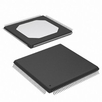
XC3S100E-4TQG144I Xilinx Inc, XC3S100E-4TQG144I Datasheet - Page 84

XC3S100E-4TQG144I
Manufacturer Part Number
XC3S100E-4TQG144I
Description
IC FPGA SPARTAN-3E 100K 144-TQFP
Manufacturer
Xilinx Inc
Series
Spartan™-3Er
Datasheet
1.XC3S100E-4TQG144I.pdf
(193 pages)
Specifications of XC3S100E-4TQG144I
Package / Case
144-TQFP, 144-VQFP
Mounting Type
Surface Mount
Voltage - Supply
1.1 V ~ 3.465 V
Operating Temperature
-40°C ~ 100°C
Number Of I /o
108
Number Of Logic Elements/cells
*
Number Of Gates
*
Lead Free Status / RoHS Status
Lead free / RoHS Compliant
Available stocks
Company
Part Number
Manufacturer
Quantity
Price
Company:
Part Number:
XC3S100E-4TQG144I
Manufacturer:
XILINX/21
Quantity:
163
Company:
Part Number:
XC3S100E-4TQG144I
Manufacturer:
Xilinx Inc
Quantity:
10 000
Part Number:
XC3S100E-4TQG144I
Manufacturer:
XILINX/赛灵思
Quantity:
20 000
- Current page: 84 of 193
- Download datasheet (2Mb)
Table 54: FPGA Connections to Flash PROM with "IO15/A-1" Pin
Daisy-Chaining
If the application requires multiple FPGAs with different con-
figurations, then configure the FPGAs using a daisy chain,
as shown in
<0:1:1>) for the FPGA connected to the parallel NOR Flash
PROM and Slave Parallel mode (M[2:0] = <1:1:0>) for all
other FPGAs in the daisy-chain. After the master
FPGA—the FPGA on the left in the diagram—finishes load-
ing its configuration data from the parallel Flash PROM, the
master device continues generating addresses to the Flash
PROM and asserts its CSO_B output Low, enabling the
DS312-2 (v1.1) March 21, 2005
Advance Product Specification
LDC2
LDC1
LDC0
HDC
A[23:1]
A0
D[7:0]
User I/O
FPGA Pin
R
Figure
BYTE#
OE#
CS#
WE#
A[n:0]
IO15/A-1
IO[7:0]
Upper data lines IO[14:8] not
required unless used as x16 Flash
interface after configuration
Connection to Flash PROM with
56. Use BPI mode (M[2:0] = <0:1:0> or
IO15/A-1 Pin
x8 Flash PROM Interface After
Drive LDC2 Low or leave
unconnected and tie PROM
BYTE# input to GND
Active-Low Flash PROM
output-enable control
Active-Low Flash PROM
chip-select control
Flash PROM write-enable
control
A[n:0]
IO15/A-1 is least-significant
address input
IO[7:0]
Upper data lines IO[14:8] not
required
www.xilinx.com
FPGA Configuration
next FPGA in the daisy-chain. The next FPGA then receives
parallel configuration data from the Flash PROM. The mas-
ter FPGA’s CCLK output synchronizes data capture.
The downstream devices in Slave Parallel mode also
actively drive their LDC[2:0] and HDC outputs during config-
uration, although these signal are not used for configura-
tion. These pins are in I/O Bank 1, powered by VCCO_1.
Because these pins do not connect elsewhere in the config-
uration circuit, the voltage on VCCO_1 can be whatever is
required by the end application.
x16 Flash PROM Interface After
Drive LCD2 High
Active-Low Flash PROM
output-enable control
Active-Low Flash PROM
chip-select control
Flash PROM write-enable control
A[n:0]
IO15/A-1 is most-significant data
line, IO15
IO[7:0]
IO[14:8]
FPGA Configuration
Functional Description
77
Related parts for XC3S100E-4TQG144I
Image
Part Number
Description
Manufacturer
Datasheet
Request
R

Part Number:
Description:
IC SPARTAN-3E FPGA 100K 144-TQFP
Manufacturer:
Xilinx Inc
Datasheet:

Part Number:
Description:
FIELD PROGRAMMER
Manufacturer:
Xilinx Inc
Datasheet:

Part Number:
Description:
FPGA Spartan®-3E Family 100K Gates 2160 Cells 572MHz 90nm (CMOS) Technology 1.2V 100-Pin VTQFP
Manufacturer:
Xilinx Inc
Datasheet:

Part Number:
Description:
FPGA Spartan®-3E Family 100K Gates 2160 Cells 572MHz 90nm (CMOS) Technology 1.2V 144-Pin TQFP
Manufacturer:
Xilinx Inc
Datasheet:

Part Number:
Description:
FPGA Spartan®-3E Family 100K Gates 2160 Cells 657MHz 90nm (CMOS) Technology 1.2V 144-Pin TQFP
Manufacturer:
Xilinx Inc
Datasheet:

Part Number:
Description:
Spartan-3E FPGA Family
Manufacturer:
XILINX [Xilinx, Inc]
Datasheet:

Part Number:
Description:
Spartan-3E FPGA Family: Complete Data Sheet
Manufacturer:
XILINX [Xilinx, Inc]
Datasheet:

Part Number:
Description:
IC FPGA SPARTAN-3E 100K 100-VQFP
Manufacturer:
Xilinx Inc
Datasheet:

Part Number:
Description:
IC FPGA SPARTAN-3E 100K 132CSBGA
Manufacturer:
Xilinx Inc
Datasheet:

Part Number:
Description:
IC FPGA SPARTAN-3E 100K 132CSBGA
Manufacturer:
Xilinx Inc
Datasheet:

Part Number:
Description:
IC FPGA SPARTAN-3E 100K 144-TQFP
Manufacturer:
Xilinx Inc
Datasheet:

Part Number:
Description:
IC FPGA SPARTAN 3E 100VQFP
Manufacturer:
Xilinx Inc
Datasheet:

Part Number:
Description:
IC FPGA SPARTAN 3E 144TQFP
Manufacturer:
Xilinx Inc
Datasheet:

Part Number:
Description:
FPGA Spartan®-3E Family 100K Gates 2160 Cells 572MHz 90nm (CMOS) Technology 1.2V 132-Pin CSBGA
Manufacturer:
Xilinx Inc
Datasheet:

Part Number:
Description:
IC CPLD .8K 36MCELL 44-VQFP
Manufacturer:
Xilinx Inc
Datasheet:


