XC3S100E-4TQG144I Xilinx Inc, XC3S100E-4TQG144I Datasheet - Page 39
XC3S100E-4TQG144I
Manufacturer Part Number
XC3S100E-4TQG144I
Description
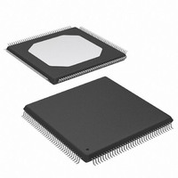
IC FPGA SPARTAN-3E 100K 144-TQFP
Manufacturer
Xilinx Inc
Series
Spartan™-3Er
Datasheet
1.XC3S100E-4TQG144I.pdf
(193 pages)
Specifications of XC3S100E-4TQG144I
Package / Case
144-TQFP, 144-VQFP
Mounting Type
Surface Mount
Voltage - Supply
1.1 V ~ 3.465 V
Operating Temperature
-40°C ~ 100°C
Number Of I /o
108
Number Of Logic Elements/cells
*
Number Of Gates
*
Lead Free Status / RoHS Status
Lead free / RoHS Compliant
Available stocks
Company
Part Number
Manufacturer
Quantity
Price
Company:

Part Number:
XC3S100E-4TQG144I
Manufacturer:
XILINX/21
Quantity:
163
Company:
Part Number:
XC3S100E-4TQG144I
Manufacturer:
Xilinx Inc
Quantity:
10 000
Part Number:
XC3S100E-4TQG144I
Manufacturer:
XILINX/赛灵思
Quantity:
20 000


Functional Description
Table 21: Block RAM Attributes (Continued)
Block RAM Data Operations
Writing data to and accessing data from the block RAM are
synchronous operations that take place independently on
each of the two ports.
tions of each port as a result of the block RAM control sig-
nals in their default active-High edges.
Table 22: Block RAM Function Table
32
Data Output Latch Synchronous
Set/Reset Value
Data Output Latch Behavior during Write
(see
GSR
1
0
0
0
0
0
Block RAM Data
EN
X
0
1
1
1
1
Loaded During Configuration
SSR
Function
X
X
1
1
0
0
Table 22
Input Signals
WE
Operations)
X
X
0
1
0
1
CLK
X
X
↑
↑
↑
↑
describes the data opera-
Global Set/Reset Immediately After Configuration
ADDR
Synchronous Set/Reset During Write RAM
Write RAM, Simultaneous Read Operation
addr
addr
addr
X
X
X
Immediately After Configuration
Read RAM, no Write Operation
pdata
pdata
DIP
SRVAL_A, SRVAL_B
Synchronous Set/Reset
SRVAL (single-port)
X
X
X
X
WRITE_MODE
(dual-port)
RAM Disabled
Attribute
www.xilinx.com
Data
Data
DI
X
X
X
X
RAM(pdata)
The waveforms for the write operation are shown in the top
half of
and EN signals enable the active edge of CLK, data at the
DI input bus is written to the block RAM location addressed
by the ADDR lines.
RAM(data)
No Chg
No Chg
SRVAL
SRVAL
pdata
DOP
INIT
X
Output Signals
Figure
Hex value the width of the chosen port.
WRITE_FIRST, READ_FIRST, NO_CHANGE
WRITE_MODE = WRITE_FIRST
WRITE_MODE = NO_CHANGE
WRITE_MODE = READ_FIRST
30,
RAM(data)
RAM(data)
No Chg
No Chg
SRVAL
SRVAL
Figure
INIT
data
DO
X
31, and
Possible Values
Advance Product Specification
RAM(addr)
RAM(addr)
RAM(addr)
RAM(addr)
DS312-2 (v1.1) March 21, 2005
INITP_xx
← pdata
← pdata
← pdata
← pdata
No Chg
No Chg
No Chg
No Chg
Parity
Figure
RAM Data
32. When the WE
RAM(addr)
RAM(addr)
RAM(addr)
RAM(addr)
← pdata
← pdata
INIT_xx
← data
← data
No Chg
No Chg
No Chg
No Chg
Data
R
Related parts for XC3S100E-4TQG144I
Image
Part Number
Description
Manufacturer
Datasheet
Request
R

Part Number:
Description:
IC SPARTAN-3E FPGA 100K 144-TQFP
Manufacturer:
Xilinx Inc
Datasheet:

Part Number:
Description:
FIELD PROGRAMMER
Manufacturer:
Xilinx Inc
Datasheet:
Part Number:
Description:
FPGA Spartan®-3E Family 100K Gates 2160 Cells 572MHz 90nm (CMOS) Technology 1.2V 100-Pin VTQFP
Manufacturer:
Xilinx Inc
Datasheet:

Part Number:
Description:
FPGA Spartan®-3E Family 100K Gates 2160 Cells 572MHz 90nm (CMOS) Technology 1.2V 144-Pin TQFP
Manufacturer:
Xilinx Inc
Datasheet:
Part Number:
Description:
FPGA Spartan®-3E Family 100K Gates 2160 Cells 657MHz 90nm (CMOS) Technology 1.2V 144-Pin TQFP
Manufacturer:
Xilinx Inc
Datasheet:
Part Number:
Description:
Spartan-3E FPGA Family
Manufacturer:
XILINX [Xilinx, Inc]
Datasheet:
Part Number:
Description:
Spartan-3E FPGA Family: Complete Data Sheet
Manufacturer:
XILINX [Xilinx, Inc]
Datasheet:
Part Number:
Description:
IC FPGA SPARTAN-3E 100K 100-VQFP
Manufacturer:
Xilinx Inc
Datasheet:

Part Number:
Description:
IC FPGA SPARTAN-3E 100K 132CSBGA
Manufacturer:
Xilinx Inc
Datasheet:
Part Number:
Description:
IC FPGA SPARTAN-3E 100K 132CSBGA
Manufacturer:
Xilinx Inc
Datasheet:
Part Number:
Description:
IC FPGA SPARTAN-3E 100K 144-TQFP
Manufacturer:
Xilinx Inc
Datasheet:
Part Number:
Description:
IC FPGA SPARTAN 3E 100VQFP
Manufacturer:
Xilinx Inc
Datasheet:
Part Number:
Description:
IC FPGA SPARTAN 3E 144TQFP
Manufacturer:
Xilinx Inc
Datasheet:
Part Number:
Description:
FPGA Spartan®-3E Family 100K Gates 2160 Cells 572MHz 90nm (CMOS) Technology 1.2V 132-Pin CSBGA
Manufacturer:
Xilinx Inc
Datasheet:

Part Number:
Description:
IC CPLD .8K 36MCELL 44-VQFP
Manufacturer:
Xilinx Inc
Datasheet: