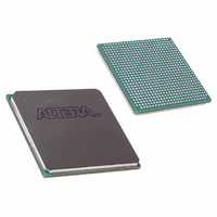
EP2S30F672C5N Altera, EP2S30F672C5N Datasheet - Page 95

EP2S30F672C5N
Manufacturer Part Number
EP2S30F672C5N
Description
IC STRATIX II FPGA 30K 672-FBGA
Manufacturer
Altera
Series
Stratix® IIr
Datasheet
1.EP2S15F484I4N.pdf
(238 pages)
Specifications of EP2S30F672C5N
Number Of Logic Elements/cells
33880
Number Of Labs/clbs
1694
Total Ram Bits
1369728
Number Of I /o
500
Voltage - Supply
1.15 V ~ 1.25 V
Mounting Type
Surface Mount
Operating Temperature
0°C ~ 85°C
Package / Case
672-FBGA
Family Name
Stratix II
Number Of Logic Blocks/elements
33880
# I/os (max)
500
Frequency (max)
609.76MHz
Process Technology
90nm (CMOS)
Operating Supply Voltage (typ)
1.2V
Logic Cells
33880
Ram Bits
1369728
Operating Supply Voltage (min)
1.15V
Operating Supply Voltage (max)
1.25V
Operating Temp Range
0C to 85C
Operating Temperature Classification
Commercial
Mounting
Surface Mount
Pin Count
672
Package Type
FC-FBGA
Family Type
Stratix II
No. Of I/o's
500
I/o Supply Voltage
3.3V
Operating Frequency Max
550MHz
Operating Temperature Range
0°C To +85°C
Logic Case Style
BGA
No. Of Pins
672
Rohs Compliant
Yes
Lead Free Status / RoHS Status
Lead free / RoHS Compliant
Number Of Gates
-
Lead Free Status / Rohs Status
Compliant
Other names
544-1898
EP2S30F672C5N
EP2S30F672C5N
Available stocks
Company
Part Number
Manufacturer
Quantity
Price
Company:
Part Number:
EP2S30F672C5N
Manufacturer:
ALTERA
Quantity:
238
Part Number:
EP2S30F672C5N
Manufacturer:
ALTERA/阿尔特拉
Quantity:
20 000
Altera Corporation
May 2007
Notes to
(1)
(2)
(3)
(4)
SSTL-2 Class I and II
Table 2–16. Stratix II Supported I/O Standards (Part 2 of 2)
This I/O standard is only available on input and output column clock pins.
This I/O standard is only available on input clock pins and DQS pins in I/O banks 3, 4, 7, and 8, and output clock
pins in I/O banks 9,10, 11, and 12.
V
The clock input pins supporting LVDS on banks 3, 4, 7, and 8 use V
dependency on the V
1.2-V HSTL is only supported in I/O banks 4,7, and 8.
CCIO
I/O Standard
Table
is 3.3 V when using this I/O standard in input and output column clock pins (in I/O banks 9, 10, 11, and 12).
2–16:
f
CCIO
Voltage-referenced
level of the bank.
For more information on I/O standards supported by Stratix II I/O
banks, refer to the Selectable I/O Standards in Stratix II & Stratix II GX
Devices chapter in volume 2 of the Stratix II Device Handbook or the
Stratix II GX Device Handbook.
Stratix II devices contain eight I/O banks and four enhanced PLL external
clock output banks, as shown in
right and left of the device contain circuitry to support high-speed
differential I/O for LVDS and HyperTransport inputs and outputs. These
banks support all Stratix II I/O standards except PCI or PCI-X I/O pins,
and SSTL-18 Class II and HSTL outputs. The top and bottom I/O banks
support all single-ended I/O standards. Additionally, enhanced PLL
external clock output banks allow clock output capabilities such as
differential support for SSTL and HSTL.
Type
Voltage (V
Input Reference
1.25
REF
) (V)
Figure
CCINT
Voltage (V
Stratix II Device Handbook, Volume 1
Output Supply
for LVDS input operations and have no
2–57. The four I/O banks on the
2.5
CCIO
) (V)
Stratix II Architecture
Board Termination
Voltage (V
1.25
TT
) (V)
2–87


