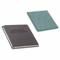
EP2S30F672C5N Altera, EP2S30F672C5N Datasheet - Page 6

EP2S30F672C5N
Manufacturer Part Number
EP2S30F672C5N
Description
IC STRATIX II FPGA 30K 672-FBGA
Manufacturer
Altera
Series
Stratix® IIr
Datasheet
1.EP2S15F484I4N.pdf
(238 pages)
Specifications of EP2S30F672C5N
Number Of Logic Elements/cells
33880
Number Of Labs/clbs
1694
Total Ram Bits
1369728
Number Of I /o
500
Voltage - Supply
1.15 V ~ 1.25 V
Mounting Type
Surface Mount
Operating Temperature
0°C ~ 85°C
Package / Case
672-FBGA
Family Name
Stratix II
Number Of Logic Blocks/elements
33880
# I/os (max)
500
Frequency (max)
609.76MHz
Process Technology
90nm (CMOS)
Operating Supply Voltage (typ)
1.2V
Logic Cells
33880
Ram Bits
1369728
Operating Supply Voltage (min)
1.15V
Operating Supply Voltage (max)
1.25V
Operating Temp Range
0C to 85C
Operating Temperature Classification
Commercial
Mounting
Surface Mount
Pin Count
672
Package Type
FC-FBGA
Family Type
Stratix II
No. Of I/o's
500
I/o Supply Voltage
3.3V
Operating Frequency Max
550MHz
Operating Temperature Range
0°C To +85°C
Logic Case Style
BGA
No. Of Pins
672
Rohs Compliant
Yes
Lead Free Status / RoHS Status
Lead free / RoHS Compliant
Number Of Gates
-
Lead Free Status / Rohs Status
Compliant
Other names
544-1898
EP2S30F672C5N
EP2S30F672C5N
Available stocks
Company
Part Number
Manufacturer
Quantity
Price
Company:
Part Number:
EP2S30F672C5N
Manufacturer:
ALTERA
Quantity:
238
Part Number:
EP2S30F672C5N
Manufacturer:
ALTERA/阿尔特拉
Quantity:
20 000
Features
1–4
Stratix II Device Handbook, Volume 1
Note to
(1)
EP2S15 to EP2S30
EP2S15 to EP2S60
EP2S30 to EP2S60
EP2S60 to EP2S90
EP2S60 to EP2S130
EP2S60 to EP2S180
EP2S90 to EP2S130
EP2S90 to EP2S180
EP2S130 to EP2S180
Table 1–4. Total Number of Non-Migratable I/O Pins for Stratix II Vertical Migration Paths
Vertical Migration
Some of the DQ/DQS pins are not migratable. Refer to the Quartus II software information messages for more
detailed information.
Table
Path
1–4:
f
FineLine BGA
484-Pin
After compilation, check the information messages for a full list of I/O,
DQ, LVDS, and other pins that are not available because of the selected
migration path.
Table 1–4
number of non-migratable user I/O pins when migrating from one
density device to a larger density device. Additional I/O pins may not be
migratable if migrating from the larger device to the smaller density
device.
1
1
Refer to the I/O Management chapter in volume 2 of the Quartus II
Handbook for more information on pin migration.
0
8
8
(1)
(1)
(1)
When moving from one density to a larger density, the larger
density device may have fewer user I/O pins. The larger device
requires more power and ground pins to support the additional
logic within the device. Use the Quartus II Pin Planner to
determine which user I/O pins are migratable between the two
devices.
To determine if your user I/O assignments are correct, run the
I/O Assignment Analysis command in the Quartus II software
(Processing > Start > Start I/O Assignment Analysis).
lists the Stratix II device package offerings and shows the total
FineLine BGA
672-Pin
0
0
8
FineLine BGA
780-Pin
0
(1)
FineLine BGA
1020-Pin
16
16
0
0
0
0
Altera Corporation
FineLine BGA
1508-Pin
May 2007
17
0
0


