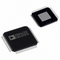
AD9775BSVRL Analog Devices Inc, AD9775BSVRL Datasheet - Page 4

AD9775BSVRL
Manufacturer Part Number
AD9775BSVRL
Description
IC DAC 14BIT DUAL 160MSPS 80TQFP
Manufacturer
Analog Devices Inc
Series
TxDAC+®r
Datasheet
1.AD9775BSVZRL.pdf
(56 pages)
Specifications of AD9775BSVRL
Rohs Status
RoHS non-compliant
Settling Time
11ns
Number Of Bits
14
Data Interface
Parallel
Number Of Converters
2
Voltage Supply Source
Analog and Digital
Power Dissipation (max)
410mW
Operating Temperature
-40°C ~ 85°C
Mounting Type
Surface Mount
Package / Case
80-TQFP Exposed Pad, 80-eTQFP, 80-HTQFP, 80-VQFP
For Use With
AD9775-EBZ - BOARD EVALUATION FOR AD9775
AD9775
GENERAL DESCRIPTION
The AD9775
compatible, high performance, programmable 2×/4×/8×
interpolating TxDAC+ family. The AD977x family features a
serial port interface (SPI) that provides a high level of
programmability, thus allowing for enhanced system-level
options. These options include selectable 2×/4×/8×
interpolation filters; f
modulation with image rejection; a direct IF mode;
programmable channel gain and offset control; programmable
internal clock divider; straight binary or twos complement data
interface; and a single-port or dual-port data interface.
The selectable 2×/4×/8× interpolation filters simplify the
requirements of the reconstruction filters while simultaneously
enhancing the pass-band noise/distortion performance of
TxDAC+ devices. The independent channel gain and offset
adjust registers allow the user to calibrate LO feedthrough and
sideband suppression errors associated with analog quadrature
modulators. The 6 dB of gain adjustment range can also be used
to control the output power level of each DAC.
The AD9775 can perform f
and image rejection when combined with an analog quadrature
modulator. In this mode, the AD9775 accepts I and Q complex
data (representing a single or multicarrier waveform), generates
a quadrature modulated IF signal along with its orthogonal
representation via its dual DACs, and presents these two
reconstructed orthogonal IF carriers to an analog quadrature
modulator to complete the image rejection upconversion
process. Another digital modulation mode (that is, the direct IF
mode) allows the original baseband signal representation to be
frequency translated such that pairs of images fall at multiples
of one-half the DAC update rate.
The AD977x family includes a flexible clock interface that
accepts differential or single-ended sine wave or digital logic
inputs. An internal PLL clock multiplier is included and
generates the necessary on-chip high frequency clocks. It can
also be disabled to allow the use of a higher performance
external clock source. An internal programmable divider
simplifies clock generation in the converter when using an
external clock source. A flexible data input interface allows for
straight binary or twos complement formats and supports
single-port interleaved or dual-port data.
Dual high performance DAC outputs provide a differential
current output programmable over a 2 mA to 20 mA range.
1
Protected by U.S. Patent Numbers 5,568,145; 5,689,257; and 5,703,519. Other patents pending.
1
is the 14-bit member of the AD977x pin-
S
/2, f
S
/4, or f
S
/2, f
S
/4, and f
S
/8 digital quadrature
S
/8 digital modulation
Rev. E | Page 4 of 56
The AD9775 is manufactured on an advanced 0.35 micron
CMOS process, operates from a single supply of 3.1 V to 3.5 V,
and consumes 1.2 W of power.
Targeted at wide dynamic range, multicarrier and multistandard
systems, the superb baseband performance of the AD9775 is
ideal for wideband CDMA, multicarrier CDMA, multicarrier
TDMA, multicarrier GSM, and high performance systems
employing high order QAM modulation schemes. The image
rejection feature simplifies and can help reduce the number of
signal band filters needed in a transmit signal chain. The direct
IF mode helps to eliminate a costly mixer stage for a variety of
communications systems.
PRODUCT HIGHLIGHTS
1.
2.
3.
4.
5.
6.
7.
8.
9.
10. Flexible clock input with single-ended or differential input,
11. Low power: complete CMOS DAC operates on 1.2 W from
12. On-chip voltage reference. The AD9775 includes a 1.20 V
13. 80-lead, thin quad flat package, exposed pad (TQFP_EP).
The AD9775 is the 14-bit member of the AD977x pin-
compatible, high performance, programmable 2×/4×/8×
interpolating TxDAC+ family.
Direct IF transmission capability for 70 MHz + IFs through
a novel digital mixing process.
f
selectable image rejection to simplify/remove cascaded
SAW filter stages.
A 2×/4×/8× user-selectable, interpolating filter eases data
rate and output signal reconstruction filter requirements.
User-selectable, twos complement/straight binary data
coding.
User-programmable, channel gain control over 1 dB range
in 0.01 dB increments.
User programmable channel offset control ±10% over the
FSR.
Ultrahigh speed 400 MSPS DAC conversion rate.
Internal clock divider provides data rate clock for easy
interfacing.
CMOS, or 1 V p-p LO sine wave input capability.
a 3.1 V to 3.5 V single supply. The 20 mA full-scale current
can be reduced for lower power operation and several sleep
functions are provided to reduce power during idle
periods.
temperature compensated band gap voltage reference.
S
/2, f
S
/4, and f
S
/8 digital quadrature modulation and user-


