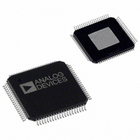
AD9775BSVRL Analog Devices Inc, AD9775BSVRL Datasheet - Page 24

AD9775BSVRL
Manufacturer Part Number
AD9775BSVRL
Description
IC DAC 14BIT DUAL 160MSPS 80TQFP
Manufacturer
Analog Devices Inc
Series
TxDAC+®r
Datasheet
1.AD9775BSVZRL.pdf
(56 pages)
Specifications of AD9775BSVRL
Rohs Status
RoHS non-compliant
Settling Time
11ns
Number Of Bits
14
Data Interface
Parallel
Number Of Converters
2
Voltage Supply Source
Analog and Digital
Power Dissipation (max)
410mW
Operating Temperature
-40°C ~ 85°C
Mounting Type
Surface Mount
Package / Case
80-TQFP Exposed Pad, 80-eTQFP, 80-HTQFP, 80-VQFP
For Use With
AD9775-EBZ - BOARD EVALUATION FOR AD9775
AD9775
DAC OPERATION
The dual, 14-bit DAC output of the AD9775, along with the
reference circuitry, gain, and offset registers, is shown in Figure 37.
Note that an external reference can be used by simply overdriving
the internal reference with the external reference. Referring to the
transfer functions in Equation 1, a reference current is set by the
internal 1.2 V reference, the external R
in the coarse gain register. The fine gain DAC subtracts a small
amount from this and the result is input to IDAC and QDAC,
where it is scaled by an amount equal to 1024/24. Figure 38 and
Figure 39 show the scaling effect of the coarse and fine adjust
DACs. IDAC and QDAC are PMOS current source arrays,
segmented in a 5-4-5 configuration. The 5 MSBs control an array
of 31 current sources. The next four bits consist of 15 current
sources whose values are all equal to 1/16 of an MSB current
source. The 5 LSBs are binary weighted fractions of the middle
bits’ current sources. All current sources are switched to either
I
The fine adjustment of the gain of each channel allows for
improved balance of QAM modulated signals, resulting in
improved modulation accuracy and image rejection.
In the section Interfacing the AD9775 with the AD8345
Quadrature Modulator, the performance data shows to what
degree image rejection can be improved when the AD9775 is
used with an AD8345 quadrature modulator from Analog
Devices, Inc.
OUTA
or I
OUTB
, depending on the input code.
Figure 37. Equivalent Internal Reference Circuit
84μA
0.7V
AVDD
7kΩ
REGISTERS
REFIO
REFIO
CONTROL
SET
Figure 40. DAC Outputs, Reference Current Scaling, and Gain/Offset Adjust
1.2VREF
0.1μF
GAIN
resistor, and the values
RSET1
FSADJ1
GAIN
GAIN
FINE
FINE
DAC
DAC
RSET2
COARSE
GAIN
FSADJ2
DAC
Rev. E | Page 24 of 56
COARSE
REGISTERS
GAIN
DAC
CONTROL
GAIN
–0.5
–1.0
–1.5
–2.0
–2.5
–3.0
REGISTERS
REGISTERS
CONTROL
IDAC
QDAC
CONTROL
0
25
20
15
10
OFFSET
OFFSET
0
5
0
0
OFFSET
OFFSET
Figure 38. Coarse Gain Effect on I
DAC
DAC
200
Figure 39. Fine Gain Effect on I
(ASSUMING RSET1, RSET2 = 1.9kΩ)
(ASSUMING RSET1, RSET2 = 1.9kΩ)
5
COARSE GAIN REGISTER CODE
I
I
I
I
OUTA1
OUTB1
OUTA2
OUTB2
FINE GAIN REGISTER CODE
2R MODE
400
10
1R MODE
600
1R MODE
2R MODE
FULLSCALE
15
FULLSCALE
800
20
1000


