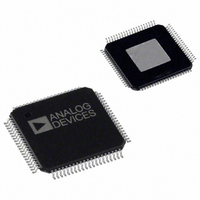
AD9775BSVRL Analog Devices Inc, AD9775BSVRL Datasheet - Page 22

AD9775BSVRL
Manufacturer Part Number
AD9775BSVRL
Description
IC DAC 14BIT DUAL 160MSPS 80TQFP
Manufacturer
Analog Devices Inc
Series
TxDAC+®r
Datasheet
1.AD9775BSVZRL.pdf
(56 pages)
Specifications of AD9775BSVRL
Rohs Status
RoHS non-compliant
Settling Time
11ns
Number Of Bits
14
Data Interface
Parallel
Number Of Converters
2
Voltage Supply Source
Analog and Digital
Power Dissipation (max)
410mW
Operating Temperature
-40°C ~ 85°C
Mounting Type
Surface Mount
Package / Case
80-TQFP Exposed Pad, 80-eTQFP, 80-HTQFP, 80-VQFP
For Use With
AD9775-EBZ - BOARD EVALUATION FOR AD9775
AD9775
INSTRUCTION BYTE
The instruction byte contains the information shown next
Table 16.
N1
0
0
1
1
R/W
Bit 7 of the instruction byte determines whether a read or a
write data transfer occurs after the instruction byte write.
Logic 1 indicates read operation. Logic 0 indicates a write
operation.
N1, N0
Bit 6 and Bit 5 of the instruction byte determine the number of
bytes to be transferred during the data transfer cycle. The bit
decodes are shown next.
Table 17.
A4, A3, A2, A1, A0
Bit 4 to Bit 0 of the instruction byte determine which register is
accessed during the data transfer portion of the communications
cycle. For multibyte transfers, this address is the starting byte
address. The remaining register addresses are generated by
the AD9775.
SERIAL INTERFACE PORT PIN DESCRIPTIONS
SPI_CLK (Pin 55)—Serial Clock
The serial clock pin is used to synchronize data to and from the
AD9775 and to run the internal state machines. SPI_CLK
maximum frequency is 15 MHz. All data input to the AD9775
is registered on the rising edge of SPI_CLK. All data is driven
out of the AD9775 on the falling edge of SPI_CLK.
SPI_CSB (Pin 56)—Chip Select
Active low input starts and gates a communication cycle. It
allows more than one device to be used on the same serial
communications lines. The SDO and SDIO pins go to a high
impedance state when this input is high. Chip select should stay
low during the entire communication cycle.
SPI_SDIO (Pin 54)—Serial Data I/O
Data is always written into the AD9775 on this pin. However,
this pin can be used as a bidirectional data line. The
configuration of this pin is controlled by Bit 7 of Register
Address 0x00. The default is Logic 0, which configures the
SDIO pin as unidirectional.
MSB
I7
R/W
I6
N1
I5
N0
N0
0
1
0
1
I4
A4
I3
A3
Description
Transfer 1 Byte
Transfer 2 Bytes
Transfer 3 Bytes
Transfer 4 Bytes
I2
A2
I1
A1
LSB
I0
A0
Rev. E | Page 22 of 56
SPI_SDO (Pin 53)—Serial Data Out
Data is read from this pin for protocols that use separate lines
for transmitting and receiving data. In the case where the
AD9775 operates in a single bidirectional I/O mode, this pin
does not output data and is set to a high impedance state.
MSB/LSB TRANSFERS
The AD9775 serial port can support both most significant bit
(MSB) first or least significant bit (LSB) first data formats. This
functionality is controlled by the LSB-first bit in Register 0. The
default is MSB first.
When this bit is set active high, the AD9775 serial port is in
LSB-first format. In LSB-first mode, the instruction byte and
data bytes must be written from LSB to MSB. In LSB-first mode,
the serial port internal byte address generator increments for
each byte of the multibyte communication cycle.
When this bit is set default low, the AD9775 serial port is in
MSB-first format. In MSB-first mode, the instruction byte and
data bytes must be written from MSB to LSB. In MSB-first
mode, the serial port internal byte address generator
decrements for each byte of the multibyte communication cycle.
When incrementing from 0x1F, the address generator changes
to 0x00. When decrementing from 0x00, the address generator
changes to 0x1F.
NOTES ON SERIAL PORT OPERATION
The AD9775 serial port configuration bits reside in Bit 6 and
Bit 7 of Register Address 0x00. It is important to note that the
configuration changes immediately upon writing to the last bit
of the register. For multibyte transfers, writing to this register
may occur during the middle of the communication cycle. Care
must be taken to compensate for this new configuration for the
remaining bytes of the current communication cycle.
The same considerations apply to setting the reset bit in
Register Address 0x00. All other registers are set to their
default values, but the software reset does not affect the bits in
Register Address 0x00.
It is recommended to use only single-byte transfers when
changing serial port configurations or initiating a software reset.
A write to Bit 1, Bit 2, and Bit 3 of Address 0x00 with the same
logic levels as for Bit 7, Bit 6, and Bit 5 (bit pattern is XY1001YX
binary) allows the user to reprogram a lost serial port
configuration and to reset the registers to their default values. A
second write to Address 0x00 with reset bit low and serial port
configuration as specified above (XY) reprograms the OSC IN
multiplier setting. A changed f
maximum of 200 f
MCLK
cycles (equals wake-up time).
SYSCLK
frequency is stable after a


