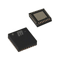
KSZ8851SNLI Micrel Inc, KSZ8851SNLI Datasheet - Page 22

KSZ8851SNLI
Manufacturer Part Number
KSZ8851SNLI
Description
Manufacturer
Micrel Inc
Datasheet
1.KSZ8851SNLI.pdf
(80 pages)
Specifications of KSZ8851SNLI
Operating Supply Voltage (typ)
3.3V
Operating Temperature Classification
Industrial
Mounting
Surface Mount
Pin Count
32
Lead Free Status / RoHS Status
Supplier Unconfirmed
Available stocks
Company
Part Number
Manufacturer
Quantity
Price
Part Number:
KSZ8851SNLI
Manufacturer:
MICROCHIP/微芯
Quantity:
20 000
Company:
Part Number:
KSZ8851SNLI TR
Manufacturer:
Kendin
Quantity:
700
Company:
Part Number:
KSZ8851SNLI TR
Manufacturer:
Micrel
Quantity:
250
Company:
Part Number:
KSZ8851SNLI-TR
Manufacturer:
MXIC
Quantity:
15 000
Company:
Part Number:
KSZ8851SNLITR
Manufacturer:
MICREL
Quantity:
3 500
Part Number:
KSZ8851SNLITR
Manufacturer:
MICREL/麦瑞
Quantity:
20 000
Clock Generator
The X1 and X2 pins are connected to a 25MHz crystal. X1 can also serve as the connector to a 3.3V, 25MHz oscillator
(as described in the pin description).
Serial Peripheral Interface (SPI)
The KSZ8851SNL supports a SPI interface in slave mode. In this mode, a external SPI master device (micro-controller or
CPU) supplies the operating serial clock (SCLK), chip select (CSN) and serial input data (SI) which is clocked in on the
rising edge of SCLK to KSZ8851SNL device. Serial output data (SO) is driven out by the KSZ8851SNL on the falling edge
of SCLK to external SPI master device. The falling edge of CSN is starting the SPI operation and the rising edge of CSN
is ending the SPI operation. The SCLK stays low state when SPI operation is idle. Figure 6 shows the SPI interface
connection for KSZ8851SNL.
There are four SPI operations depending on the opcode inside the command phase:
As shown in Table 4 and 5, there are two phases in each SPI operation, the first is command phase and the following is
data phase. Command phase is two bytes long for internal I/O registers access and one byte long for TXQ/RXQ FIFOs
access. Data phase on internal I/O registers access is in the range of one to four bytes long depending on the specified
byte enable bits B[3:0] in command phase, and data phase on TXQ or RXQ FIFOs access is limited up to 6 Kbytes for
TXQ access or 12 Kbytes for RXQ access.
August 2009
Micrel, Inc.
•
•
•
•
Note: In Command phase, A[7:2] access register address location in double word and B[3:0] enable which byte to
access during read or write. In Data phase, the byte 0 is first in/out and byte 3 is last in/out during read or write.
B[3:0] -> 1: enable byte, 0: disable byte.
Register Read
Register Write
Internal I/O registers read (opcode = 00)
Internal I/O registers write (opcode = 01)
RXQ FIFO read to receive packet (opcode = 10)
TXQ FIFO write to transmit packet (opcode = 11)
Internal I/O
Internal I/O
Operation
SPI
Opcode Byte enable
0 0
0 1
Byte 0 [7:0]
B3 B2 B1 B0 A7 A6 A5 A4 A3 A2
B3 B2 B1 B0 A7 A6 A5 A4 A3 A2
Command Phase (SI pin)
Table 4. SPI Operation for Registers Access
Figure 6. SPI Interface to KSZ8851SNL
Register Address
Byte 1 [7:0]
Don’t care bits
22
X X X X
X X X X
(read data on SO pin)
(write data on SI pin)
(SO or SI pins)
Data Phase
1 to 4 Bytes
1 to 4 Bytes
KSZ8851SNL/SNLI
M9999-083109-2.0


