KSZ8851SNLI Micrel Inc, KSZ8851SNLI Datasheet
KSZ8851SNLI
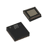
Specifications of KSZ8851SNLI
Available stocks


Related parts for KSZ8851SNLI


KSZ8851SNLI Summary of contents
Page 1
... The KSZ8851SNL is designed to be fully compliant with the appropriate IEEE 802.3 standards. An industrial temperature-grade version of the KSZ8851SNL, the KSZ8851SNLI is also available (see “Ordering Information” section). Functional Diagram LinkMD is a registered trademark of Micrel, Inc. Magic Packet is a trademark of Advanced Micro Devices, Inc. ...
Page 2
Micrel, Inc. Features • Integrated MAC and PHY Ethernet Controller fully compliant with IEEE 802.3/802.3u standards • SPI Interface with clock speeds up to 40MHz for high throughput applications • Supports 10BASE-T/100BASE-TX • Supports IEEE 802.3x full-duplex flow control and ...
Page 3
... Micrel, Inc. Ordering Information Part Number Temperature Range KSZ8851SNL TR KSZ8851SNLI TR –40 KSZ8851SNL-Eval Evaluation Board for the KSZ8851SNL Revision History Revision Date 1.0 06/30/2008 1.1 2/13/2009 2.0 8/31/2009 August 2009 Package 32-Pin MLF +85 C 32-Pin MLF Summary of Changes First released Information. Improved EDS Rating up to 6KV, revised Ordering Information and updated Table content and description ...
Page 4
Micrel, Inc. Contents Pin Configuration ................................................................................................................................................................ 10 Pin Description .................................................................................................................................................................... 11 Strapping Options ............................................................................................................................................................... 12 Functional Description ....................................................................................................................................................... 13 Functional Overview ........................................................................................................................................................... 13 Power Management........................................................................................................................................................ 13 Normal Operation Mode........................................................................................................................................... 13 Energy Detect Mode ................................................................................................................................................ 13 Soft Power Down Mode ........................................................................................................................................... ...
Page 5
Micrel, Inc. Driver Routine for Transmit Packet from Host Processor to KSZ8851SNL............................................................. 26 Receive Queue (RXQ) Frame Format ..................................................................................................................... 29 Frame Receiving Path Operation in RXQ ................................................................................................................ 29 Driver Routine for Receive Packet from KSZ8851SNL to Host Processor.............................................................. 30 EEPROM ...
Page 6
Micrel, Inc. Wakeup Frame 2 Byte Mask 1 Register (0x56 – 0x57): WF2BM1 ................................................................................ 46 Wakeup Frame 2 Byte Mask 2 Register (0x58 – 0x59): WF2BM2 ................................................................................ 46 Wakeup Frame 2 Byte Mask 3 Register (0x5A – 0x5B): WF2BM3................................................................................ 47 ...
Page 7
Micrel, Inc. Indirect Access Data Low Register (0xD0 – 0xD1): IADLR............................................................................................ 60 Indirect Access Data High Register (0xD2 – 0xD3): IADHR .......................................................................................... 60 Power Management Event Control Register (0xD4 – 0xD5): PMECR........................................................................... 60 Go-Sleep & Wake-Up Time Register (0xD6 – ...
Page 8
Micrel, Inc. List of Figures Figure 1. KSZ8851SNL/SNLI Functional Diagram.................................................................................................................. 1 Figure 2. 32-Pin (5mm x 5mm) MLF Figure 3. Typical Straight Cable Connection ........................................................................................................................ 17 Figure 4. Typical Crossover Cable Connection .................................................................................................................... 18 Figure 5. Auto Negotiation and Parallel ...
Page 9
Micrel, Inc. List of Tables Table 1. Internal Function Blocks Status .............................................................................................................................. 13 Table 2. MDI/MDI-X Pin Definitions ...................................................................................................................................... 17 Table 3. Address Filtering Scheme....................................................................................................................................... 21 Table 4. SPI Operation for Registers Access ....................................................................................................................... 22 Table 5. SPI Operation for ...
Page 10
Micrel, Inc. Pin Configuration August 2009 Figure 2. 32-Pin (5mm x 5mm) MLF 10 KSZ8851SNL/SNLI ® M9999-083109-2.0 ...
Page 11
Micrel, Inc. Pin Description Pin Number Pin Name Type 1 LED0 Opu 2 PME Opu 3 INTRN Opu 4 DGND Gnd 5 VDD_CO1.8 6 EED_IO Ipd/O 7 EESK Opd 8 AGND Gnd 9 VDD_A1.8 10 EECS Opd 11 RXP I/O ...
Page 12
Micrel, Inc. Pin Number Pin Name Type DGND Gnd 23 VDD_D1.8 24 DGND Gnd 25 VDD_IO 26 CSN Ipu SCLK 29 DGND Gnd 30 VDD_IO 31 SI Ipd 32 LED1 Opu Legend: ...
Page 13
Micrel, Inc. Functional Description The KSZ8851SNL is a single-chip Fast Ethernet MAC/PHY controller consisting of a 10/100 physical layer transceiver (PHY), a MAC, and an industry standard Serial Peripheral Interface (SPI). The host CPU is via SPI interface to read/write ...
Page 14
Micrel, Inc. The KSZ8851SNL will also assert PME output pin if the corresponding enable bit[8] is set in PMECR (0xD4) register or generate interrupt to signal an energy detect event occurred if the corresponding enable bit[2] is set in IER ...
Page 15
Micrel, Inc. Wake-up Packet Wake-up packets are certain types of packets with specific CRC values that a system recognizes as a ‘wake up’ frame. The KSZ8851SNL supports up to four users defined wake-up frames as below: 1. Wake-up frame 0 ...
Page 16
Micrel, Inc. Physical Layer Transceiver (PHY) 100BASE-TX Transmit The 100BASE-TX transmit function performs parallel-to-serial conversion, 4B/5B coding, scrambling, NRZ-to-NRZI conversion, and MLT3 encoding and transmission. The circuitry starts with a parallel-to-serial conversion, which converts the MII data from the MAC ...
Page 17
Micrel, Inc. MDI/MDI-X Auto Crossover To eliminate the need for crossover cables between similar devices, the KSZ8851SNL supports HP-Auto MDI/MDI-X and IEEE 802.3u standard MDI/MDI-X auto crossover. HP-Auto MDI/MDI-X is the default. The auto-sense function detects remote transmit and receive ...
Page 18
Micrel, Inc. Auto Negotiation The KSZ8851SNL conforms to the auto negotiation protocol as described by the 802.3 committee to allow the port to operate at either 10Base-T or 100Base-TX. Auto negotiation allows unshielded twisted pair (UTP) link partners to select ...
Page 19
Micrel, Inc. Start Auto Negotiation Force Link Setting YES and Set Link Mode ® LinkMD Cable Diagnostics ® The ...
Page 20
Micrel, Inc. Usage ® LinkMD can be run at any time by ensuring that Auto-MDIX has been disabled. To disable Auto-MDIX, write a ‘1’ to P1CR[10] to enable manual control over the pair used to transmit the LinkMD test enable ...
Page 21
Micrel, Inc. transmitter on) with zero pause time to turn off the flow control (turn on transmission to the port). A hysteresis feature is provided to prevent the flow control mechanism from being constantly activated and deactivated. Half-Duplex Backpressure A ...
Page 22
Micrel, Inc. Clock Generator The X1 and X2 pins are connected to a 25MHz crystal. X1 can also serve as the connector to a 3.3V, 25MHz oscillator (as described in the pin description). Serial Peripheral Interface (SPI) The KSZ8851SNL supports ...
Page 23
Micrel, Inc. SPI Operation RXQ FIFO Read (12 KByte) TXQ FIFO Write (6 KByte) Note: The Start DMA Access bit 3 in RXQCR register must set to “1” before FIFO read/write commands. This bit must be clear to “0” when ...
Page 24
Micrel, Inc. 0 contains only opcode (10: read command, 11: write command) and the following is read/write data phase. CSN SCLK High Impedance SO RXQ Read Command Byte 0 CSN SCLK ...
Page 25
Micrel, Inc. for the frame to transmit. The second word is used to specify the total number of bytes of the frame. The packet data follows. The packet data area holds the frame itself. It may or may not include ...
Page 26
Micrel, Inc. Register Name Description [bit](offset) TXCR[3:0](0x70) Set transmit control function as below: TXCR[8:5](0x70) Set bit 3 to enable transmitting flow control. Set bit 2 to enable transmitting padding. Set bit 1 to enable transmitting CRC. Set bit 0 to ...
Page 27
Micrel, Inc. Host receives an Ethernet pkt from upper layer and prepares transmit pkt data (data, data_length, frame ID). The transmit queue frame format is Check if KSZ8851SNL TXQ Memory size is available for this Write an 1?to RXQCR[3] reg ...
Page 28
Micrel, Inc. Host receives an multiple Ethernet pkts from upper layer and prepares transmit pkts data (data, data_length, frame ID). Each transmit queue frame format is shown in Table 6 Write an 1?to TXQCR[2] reg to issue a transmit command ...
Page 29
Micrel, Inc. Receive Queue (RXQ) Frame Format The frame format for the receive queue is shown in Table 10. The first word contains the status information for the frame received. The second word is the total number of bytes of ...
Page 30
Micrel, Inc. Driver Routine for Receive Packet from KSZ8851SNL to Host Processor The software driver receives data packet frames from the KSZ8851SNL device either as a result of polling or an interrupt based service. When an interrupt is received, the ...
Page 31
Micrel, Inc. In order to read received frames from RXQ without error, the software driver must use following steps: 1. When receive interrupt occurred and software driver writes “1” to clear the RX interrupt in ISR register; the KSZ8851 will ...
Page 32
Micrel, Inc. Loopback Support The KSZ8851SNL provides two loopback modes, one is Near-end (Remote) loopback to support for remote diagnostic of failure at line side, and the other is Far-end (Local) loopback to support for local diagnostic of failure at ...
Page 33
Micrel, Inc. SPI Interface to I/O Registers The KSZ8851SNL provides a SPI interface for the host CPU to access its internal I/O registers. I/O registers serve as the address that the microprocessor uses when communicating with the device. This is ...
Page 34
Micrel, Inc. Internal I/O Registers Space Mapping I/O Register Offset Location 32-Bit 16-Bit 0x00 - 0x01 0x00 to 0x03 0x02 - 0x03 0x04 - 0x05 0x04 to 0x07 0x06 - 0x07 0x08 - 0x09 0x08 to 0x0B 0x0A - 0x0B ...
Page 35
Micrel, Inc. I/O Register Offset Location 32-Bit 16-Bit 0x30 - 0x31 0x30 to 0x33 0x32 - 0x33 0x34 - 0x35 0x34 to 0x37 0x36 - 0x37 0x38 - 0x39 0x38 to 0x3B 0x3A - 0x3B 0x3C - 0x3D 0x3C To ...
Page 36
Micrel, Inc. I/O Register Offset Location 32-Bit 16-Bit 0x60 - 0x61 0x60 to 0x63 0x62 - 0x63 0x64 - 0x65 0x64 to 0x67 0x66 - 0x67 0x68 - 0x69 0x68 to 0x6B 0x6A - 0x6B 0x6C - 0x6D 0x6C to ...
Page 37
Micrel, Inc. I/O Register Offset Location 32-Bit 16-Bit 0x90 - 0x91 0x90 to 0x93 0x92 - 0x93 0x94 0x94 - 0x95 to 0x97 0x96 - 0x97 0x98 - 0x99 0x98 to 0x9B 0x9A - 0x9B 0x9C - 0x9D 0x9C to ...
Page 38
Micrel, Inc. I/O Register Offset Location 32-Bit 16-Bit 0xC0 - 0xC1 0xC0 to 0xC3 0xC2 - 0xC3 0xC4 - 0xC5 0xC4 to 0xC7 0xC6 - 0xC7 0xC8 - 0xC9 0xC8 to 0xCB 0xCA - 0xCB 0xCC - 0xCD 0xCC to ...
Page 39
Micrel, Inc. I/O Register Offset Location 32-Bit 16-Bit 0xF0 0xF0 - 0xF1 to 0xF3 0xF2 - 0xF3 0xF4 - 0xF5 0xF4 to 0xF7 0xF6 - 0xF7 0xF8 0xF8 - 0xF9 to 0xFB 0xFA - 0xFB 0xFC 0xFC - 0xFD to ...
Page 40
Micrel, Inc. Register Map: MAC, PHY and QMU Do not write to bit values or to registers defined as Reserved. Manipulating reserved bits or registers causes unpredictable and often fatal results. If the user wants to write to these reserved ...
Page 41
Micrel, Inc. MARH[15:0] = 0x0123 Host MAC Address Register Low (0x10 – 0x11): MARL The following table shows the register bit fields for Low word of Host MAC address. Bit Default Value R/W 15 Host MAC Address Register ...
Page 42
Micrel, Inc. EEPROM Control Register (0x22 – 0x23): EEPCR To support an external EEPROM, pulled-up the EED_IO pin to High; otherwise pulled-down to Low external EEPROM is not used, the software programs the host MAC address. ...
Page 43
Micrel, Inc. Global Reset Register (0x26 – 0x27): GRR This register controls the global and QMU reset functions with information programmed by the CPU. Bit Default Value R/W 15-2 0x0000 0x28 – 0x29: ...
Page 44
Micrel, Inc. The value of the CRC calculated is based on the IEEE 802.3 Ethernet standard taken over the bytes specified in the wake up byte mask registers. Bit Default Value R/W 15-0 0x0000 RW Wakeup Frame 0 ...
Page 45
Micrel, Inc. 0x3C – 0x3F: Reserved Wakeup Frame 1 CRC0 Register (0x40 – 0x41): WF1CRC0 This register contains the expected CRC values of the Wake up frame 1 pattern. The value of the CRC calculated is based on the IEEE ...
Page 46
Micrel, Inc. Bit Default Value R/W 15-0 0x0000 RW 0x4C – 0x4F: Reserved Wakeup Frame 2 CRC0 Register (0x50 – 0x51): WF2CRC0 This register contains the expected CRC values of the Wake up frame 2 pattern. The value of the ...
Page 47
Micrel, Inc. Wakeup Frame 2 Byte Mask 3 Register (0x5A – 0x5B): WF2BM3 This register contains the last 16 bytes mask values of the Wake up frame 2 pattern. Setting bit 0 selects the 49th byte of the Wake up ...
Page 48
Micrel, Inc. Wakeup Frame 3 Byte Mask 3 Register (0x6A – 0x6B): WF3BM3 This register contains the last 16 bytes mask values of the Wake up frame 3 pattern. Setting bit 0 selects the 49th byte of the Wake up ...
Page 49
Micrel, Inc. Bit Default Value R/W 15-14 0x0 RO 13 0x0 RO 12 0x0 Receive Control Register 1 (0x74 – 0x75): RXCR1 This register holds control information programmed by the CPU to control ...
Page 50
Micrel, Inc. Bit Default Value R/W 6 0x0 RW 5 0x0 RW 4 0x0 RW 3 0x0 RW 2 0x0 RW 1 0x0 RW 0 0x0 RW Receive Control Register 2 (0x76 – 0x77): RXCR2 This register holds control information ...
Page 51
Micrel, Inc. Bit Default Value R/W 1 0x0 RW 0 0x0 RW TXQ Memory Information Register (0x78 – 0x79): TXMIR This register indicates the amount of free memory available in the TXQ of the QMU module. Bit Default Value R/W ...
Page 52
Micrel, Inc. Bit Default Value R Receive Frame Header Byte Count Register (0x7E – 0x7F): RXFHBCR This register indicates the received frame header byte count information, the received ...
Page 53
Micrel, Inc. RXQ Command Register (0x82 – 0x83): RXQCR This register is programmed by the Host CPU to issue DMA read or write command to the RXQ and TXQ. This register also is used to control all RX thresholds enable ...
Page 54
Micrel, Inc. Bit Default Value R/W 0 0x0 RW TX Frame Data Pointer Register (0x84 – 0x85): TXFDPR The value of this register determines the address to be accessed within the TXQ frame buffer. When the AUTO increment is set, ...
Page 55
Micrel, Inc. 0x88 – 0x8B: Reserved RX Duration Timer Threshold Register (0x8C – 0x8D): RXDTTR This register is used to program the received frame duration timer threshold. Bit Default Value R/W 15-0 0x0000 RW RX Data Byte Count Threshold Register ...
Page 56
Micrel, Inc. Bit Default Value R/W 4 0x0 RW 3 0x0 RW 2 0x0 RW 1 0x0 RW 0 0x0 RW Interrupt Status Register (0x92 – 0x93): ISR This register contains the status bits for all QMU and other interrupt ...
Page 57
Micrel, Inc. Bit Default Value R/W 6 0x0 RO (W1C) 5 0x0 RO 4 0x0 RO 3 0x0 RO 2 0x0 RO 1 0x0 RO (W1C) 0 0x0 RO 0x94 – 0x9B: Reserved RX Frame Count & Threshold Register (0x9C ...
Page 58
Micrel, Inc. MAC Address Hash Table Register 0 (0xA0 – 0xA1): MAHTR0 The 64-bit MAC address table is used for group address filtering and it is enabled by selecting item 5 “Hash perfect” mode in Table 3 (Address Filtering Scheme). ...
Page 59
Micrel, Inc. Flow Control High Watermark Register (0xB2 – 0xB3): FCHWR This register is used to control the flow control for high watermark in QMU RX queue. Bit Default Value R/W 15- 11-0 0x0300 RW Flow Control Overrun ...
Page 60
Micrel, Inc. Bit Default R/W 15-13 0x0 RW 12 0x0 RW 11-10 0x0 RW 9 4-0 0x00 RW 0xCA – 0xCF: Reserved Indirect Access Data Low Register (0xD0 – 0xD1): IADLR This register contains the indirect data (low ...
Page 61
Micrel, Inc. Bit Default Value R 5-2 0x0 RO (W1C) 1-0 0x0 RW Go-Sleep & Wake-Up Time Register (0xD6 – 0xD7): GSWUTR This register contains the value which is used to control minimum Go-Sleep ...
Page 62
Micrel, Inc. Bit Default R/W 7-0 0x0C RW PHY Reset Register (0xD8 – 0xD9): PHYRR This register contains a control bit to reset PHY block when write an “1”. Bit Default R/W 15 (Self clear) ...
Page 63
Micrel, Inc. Bit Default R PHY 1 MII-Register Basic Status Register (0xE6 – 0xE7): P1MBSR This register contains the MII register status for the chip function. Bit Default ...
Page 64
Micrel, Inc. PHY 1 PHY ID Low Register (0xE8 – 0xE9): PHY1ILR This register contains the PHY ID (low) for the chip. Bit Default R/W 15-0 0x1430 RO PHY 1 PHY ID High Register (0xEA – 0xEB): PHY1IHR This register ...
Page 65
Micrel, Inc. Bit Default R 12-11 0x0 4-0 0x01 RO 0xF0 – 0xF3: Reserved Port 1 PHY Special ...
Page 66
Micrel, Inc. Port 1 Control Register (0xF6 – 0xF7): P1CR This register contains the global per port control for the chip function. Bit Default R ...
Page 67
Micrel, Inc. Bit Default R Port 1 Status Register (0xF8 – 0xF9): P1SR This register contains the PHY port status for the chip function. Bit Default R 12-11 ...
Page 68
Micrel, Inc. Bit Default R/W 0xFA – 0xFF: Reserved August 2009 Description 1 = link partner 10BT half-duplex capable link partner not 10BT half-duplex capable. 68 KSZ8851SNL/SNLI Bit is same as: M9999-083109-2.0 ...
Page 69
Micrel, Inc. MIB (Management Information Base) Counters The KSZ8851SNL provides 32 MIB counters to monitor the port activity for network management. The MIB counters are formatted as shown below. Bit Name R/W 31-0 Counter values RO Ethernet port MIB counters ...
Page 70
Micrel, Inc. Offset Counter Name 0x1C TxTotalCollision 0x1D TxExcessiveCollision 0x1E TxSingleCollision 0x1F TxMultipleCollision Example: 1. MIB Counter Read (read port 1 “Rx64Octets” counter at indirect address offset 0x0E) Write to reg. IACR (0xC8) with 0x1C0E (set indirect address and trigger ...
Page 71
Micrel, Inc. Absolute Maximum Ratings Supply Voltage (VDD_A3.3, VDD_IO) ......... –0.5V to +4.0V Input Voltage (All Inputs).............................. –0.5V to +4.0V Output Voltage (All Outputs) ........................ –0.5V to +4.0V Lead Temperature (soldering, 20sec.) ....................... 260°C Storage Temperature (T ) ......................... –65°C ...
Page 72
Micrel, Inc. Electrical Characteristics Symbol Parameter 100BaseTX Transmit (measured differentially after 1:1 transformer) V Peak Differential Output Voltage O V Output Voltage Imbalance imb Rise/Fall Time r, f Rise/Fall Time Imbalance Duty Cycle Distortion Overshoot V Reference ...
Page 73
Micrel, Inc. Timing Specifications SPI Input and Output Timing CSN t1 SCLK t2 MSB bit SI SO CSN SCLK LSB in Symbol Parameter fSCLK SPI Clock Frequency t1 CSN active setup time t2 SI data input ...
Page 74
Micrel, Inc. Auto Negotiation Timing Timing Parameter t BTB t FLPW CTD t CTC August 2009 Figure 17. Auto Negotiation Timing Description FLP burst to FLP burst FLP burst width Clock/Data pulse width Clock pulse to data ...
Page 75
Micrel, Inc. Reset Timing As long as the stable supply voltages to reset High timing (minimum of 10ms) are met, there is no power-sequencing requirement for the KSZ8851SNL supply voltages (3.3V). The reset timing requirement is summarized in the Figure ...
Page 76
Micrel, Inc. EEPROM Timing ...
Page 77
Micrel, Inc. Selection of Isolation Transformers A 1:1 isolation transformer is required at the line interface. An isolation transformer with integrated common-mode choke is recommended for exceeding FCC requirements. Table 20 gives recommended transformer characteristics. Parameter Turns ratio Open-circuit inductance ...
Page 78
Micrel, Inc. Package Information Figure 20. 32-Pin (5mm x 5mm) MLF August 2009 ® (QFN per JDEC) Package 78 KSZ8851SNL/SNLI M9999-083109-2.0 ...
Page 79
Micrel, Inc. Acronyms and Glossary BIU Bus Interface Unit BPDU Bridge Protocol Data Unit CMOS Complementary Metal Oxide Semiconductor CRC Cyclic Redundancy Check Cut-through Switch DA Destination Address DMA Direct Memory Access EEPROM Electronically Erasable Programmable Read-only Memory EISA Extended ...
Page 80
Micrel, Inc. MDI-X Medium Dependent Interface Crossover MIB Management Information Base MII Media Independent Interface NIC Network Interface Card NPVID Non Port VLAN ID PLL Phase-Locked Loop PME Power Management Event QMU Queue Management Unit SA Source Address TDR Time ...