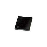
PIC18F44K20-E/MV Microchip Technology, PIC18F44K20-E/MV Datasheet - Page 402

PIC18F44K20-E/MV
Manufacturer Part Number
PIC18F44K20-E/MV
Description
16KB, Flash, 768bytes-RAM, 36I/O, 8-bit Family,nanowatt XLP 40 UQFN 5x5x0.5mm TU
Manufacturer
Microchip Technology
Series
PIC® XLP™ 18Fr
Datasheet
1.PIC18F25K20T-ISS.pdf
(456 pages)
Specifications of PIC18F44K20-E/MV
Processor Series
PIC18
Core
PIC18F
Data Bus Width
8 bit
Program Memory Type
Flash
Program Memory Size
8 KB
Data Ram Size
512 B
Interface Type
I2C, SPI, SCI, USB, MSSP, RJ11
Maximum Clock Frequency
64 MHz
Number Of Programmable I/os
35
Number Of Timers
4
Operating Supply Voltage
1.8 V to 3.6 V
Maximum Operating Temperature
+ 125 C
Mounting Style
SMD/SMT
Package / Case
UQFN-40
Development Tools By Supplier
MPLAB Integrated Development Environment
Minimum Operating Temperature
- 40 C
Operating Temperature Range
- 40 C to + 125 C
Supply Current (max)
30 uA
Core Processor
PIC
Core Size
8-Bit
Speed
48MHz
Connectivity
I²C, SPI, UART/USART
Peripherals
Brown-out Detect/Reset, HLVD, POR, PWM, WDT
Number Of I /o
35
Eeprom Size
256 x 8
Ram Size
768 x 8
Voltage - Supply (vcc/vdd)
1.8 V ~ 3.6 V
Data Converters
A/D 14x10b
Oscillator Type
Internal
Operating Temperature
-40°C ~ 125°C
Lead Free Status / Rohs Status
Details
- Current page: 402 of 456
- Download datasheet (4Mb)
PIC18F2XK20/4XK20
FIGURE 26-22:
TABLE 26-25: A/D CONVERSION REQUIREMENTS
DS41303G-page 402
130
131
132
135
136
Legend: TBD = To Be Determined
Note 1:
Param
No.
Note 1:
2:
3:
4:
A/D DATA
SAMPLE
A/D CLK
T
T
T
T
T
ADRES
Symbol
AD
CNV
ACQ
SWC
BSF ADCON0, GO
DIS
ADIF
The time of the A/D clock period is dependent on the device frequency and the T
ADRES register may be read on the following T
The time for the holding capacitor to acquire the “New” input voltage when the voltage changes full scale
after the conversion (V
.
On the following cycle of the device clock.
GO
2:
Q4
If the A/D clock source is selected as RC, a time of T
This allows the SLEEP instruction to be executed.
This is a minimal RC delay (typically 100 ns), which also disconnects the holding capacitor from the analog input.
A/D Clock Period
Conversion Time
(not including acquisition time) (Note 2)
Acquisition Time (Note 3)
Switching Time from Convert Sample
Discharge Time
132
A/D CONVERSION TIMING
(Note 2)
Characteristic
DD
9
to V
SS
8
or V
OLD_DATA
SS
7
to V
.. .
SAMPLING STOPPED
DD
CY
). The source impedance (R
CY
is added before the A/D clock starts.
cycle.
. . .
131
130
Min
0.7
0.7
1.0
1.4
12
—
2
2
(Note 4)
25.0
4.0
Max
4.0
12
—
2
(1)
(1)
1
Units
T
T
s
s
s
s
AD
AD
S
2010 Microchip Technology Inc.
) on the input channels is 50
0
T
-40C to +85C
T
+85C to +125C
FRC mode, V
V
OSC
OSC
DD
AD
= 3V, Rs = 50
based,
based,
clock divider.
NEW_DATA
DONE
Conditions
T
DD
CY
2.0V
Related parts for PIC18F44K20-E/MV
Image
Part Number
Description
Manufacturer
Datasheet
Request
R

Part Number:
Description:
Manufacturer:
Microchip Technology Inc.
Datasheet:

Part Number:
Description:
Manufacturer:
Microchip Technology Inc.
Datasheet:

Part Number:
Description:
Manufacturer:
Microchip Technology Inc.
Datasheet:

Part Number:
Description:
Manufacturer:
Microchip Technology Inc.
Datasheet:

Part Number:
Description:
Manufacturer:
Microchip Technology Inc.
Datasheet:

Part Number:
Description:
Manufacturer:
Microchip Technology Inc.
Datasheet:

Part Number:
Description:
Manufacturer:
Microchip Technology Inc.
Datasheet:

Part Number:
Description:
Manufacturer:
Microchip Technology Inc.
Datasheet:


