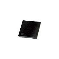
PIC18F44K20-E/MV Microchip Technology, PIC18F44K20-E/MV Datasheet - Page 156

PIC18F44K20-E/MV
Manufacturer Part Number
PIC18F44K20-E/MV
Description
16KB, Flash, 768bytes-RAM, 36I/O, 8-bit Family,nanowatt XLP 40 UQFN 5x5x0.5mm TU
Manufacturer
Microchip Technology
Series
PIC® XLP™ 18Fr
Datasheet
1.PIC18F25K20T-ISS.pdf
(456 pages)
Specifications of PIC18F44K20-E/MV
Processor Series
PIC18
Core
PIC18F
Data Bus Width
8 bit
Program Memory Type
Flash
Program Memory Size
8 KB
Data Ram Size
512 B
Interface Type
I2C, SPI, SCI, USB, MSSP, RJ11
Maximum Clock Frequency
64 MHz
Number Of Programmable I/os
35
Number Of Timers
4
Operating Supply Voltage
1.8 V to 3.6 V
Maximum Operating Temperature
+ 125 C
Mounting Style
SMD/SMT
Package / Case
UQFN-40
Development Tools By Supplier
MPLAB Integrated Development Environment
Minimum Operating Temperature
- 40 C
Operating Temperature Range
- 40 C to + 125 C
Supply Current (max)
30 uA
Core Processor
PIC
Core Size
8-Bit
Speed
48MHz
Connectivity
I²C, SPI, UART/USART
Peripherals
Brown-out Detect/Reset, HLVD, POR, PWM, WDT
Number Of I /o
35
Eeprom Size
256 x 8
Ram Size
768 x 8
Voltage - Supply (vcc/vdd)
1.8 V ~ 3.6 V
Data Converters
A/D 14x10b
Oscillator Type
Internal
Operating Temperature
-40°C ~ 125°C
Lead Free Status / Rohs Status
Details
- Current page: 156 of 456
- Download datasheet (4Mb)
PIC18F2XK20/4XK20
12.1
Timer0 can operate as either a timer or a counter; the
mode is selected with the T0CS bit of the T0CON
register. In Timer mode (T0CS = 0), the module
increments on every clock by default unless a different
prescaler
“Prescaler”). Timer0 incrementing is inhibited for two
instruction cycles following a TMR0 register write. The
user can work around this by adjusting the value written
to the TMR0 register to compensate for the anticipated
missing increments.
The Counter mode is selected by setting the T0CS bit
(= 1). In this mode, Timer0 increments either on every
rising or falling edge of pin RA4/T0CKI. The increment-
ing edge is determined by the Timer0 Source Edge
Select bit, T0SE of the T0CON register; clearing this bit
selects the rising edge. Restrictions on the external
clock input are discussed below.
An external clock source can be used to drive Timer0;
however, it must meet certain requirements (see
Table 26-11) to ensure that the external clock can be
synchronized with the internal phase clock (T
There is a delay between synchronization and the
onset of incrementing the timer/counter.
FIGURE 12-1:
DS41303G-page 156
Note:
T0CKI pin
Timer0 Operation
value
Upon Reset, Timer0 is enabled in 8-bit mode with clock input from T0CKI max. prescale.
T0SE
T0CS
T0PS<2:0>
PSA
is
F
OSC
TIMER0 BLOCK DIAGRAM (8-BIT MODE)
selected
/4
0
1
(see
Programmable
Prescaler
Section 12.3
3
OSC
).
0
1
(2 T
Sync with
Internal
Clocks
CY
12.2
TMR0H is not the actual high byte of Timer0 in 16-bit
mode; it is actually a buffered version of the real high
byte of Timer0 which is neither directly readable nor
writable (refer to Figure 12-2). TMR0H is updated with
the contents of the high byte of Timer0 during a read of
TMR0L. This provides the ability to read all 16 bits of
Timer0 without the need to verify that the read of the
high and low byte were valid. Invalid reads could
otherwise occur due to a rollover between successive
reads of the high and low byte.
Similarly, a write to the high byte of Timer0 must also
take place through the TMR0H Buffer register. Writing
to TMR0H does not directly affect Timer0. Instead, the
high byte of Timer0 is updated with the contents of
TMR0H when a write occurs to TMR0L. This allows all
16 bits of Timer0 to be updated at once.
Delay)
Timer0 Reads and Writes in
16-Bit Mode
8
TMR0L
8
2010 Microchip Technology Inc.
Set
TMR0IF
on Overflow
Internal Data Bus
Related parts for PIC18F44K20-E/MV
Image
Part Number
Description
Manufacturer
Datasheet
Request
R

Part Number:
Description:
Manufacturer:
Microchip Technology Inc.
Datasheet:

Part Number:
Description:
Manufacturer:
Microchip Technology Inc.
Datasheet:

Part Number:
Description:
Manufacturer:
Microchip Technology Inc.
Datasheet:

Part Number:
Description:
Manufacturer:
Microchip Technology Inc.
Datasheet:

Part Number:
Description:
Manufacturer:
Microchip Technology Inc.
Datasheet:

Part Number:
Description:
Manufacturer:
Microchip Technology Inc.
Datasheet:

Part Number:
Description:
Manufacturer:
Microchip Technology Inc.
Datasheet:

Part Number:
Description:
Manufacturer:
Microchip Technology Inc.
Datasheet:


