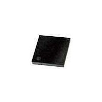
PIC18F44K20-E/MV Microchip Technology, PIC18F44K20-E/MV Datasheet - Page 289

PIC18F44K20-E/MV
Manufacturer Part Number
PIC18F44K20-E/MV
Description
16KB, Flash, 768bytes-RAM, 36I/O, 8-bit Family,nanowatt XLP 40 UQFN 5x5x0.5mm TU
Manufacturer
Microchip Technology
Series
PIC® XLP™ 18Fr
Datasheet
1.PIC18F25K20T-ISS.pdf
(456 pages)
Specifications of PIC18F44K20-E/MV
Processor Series
PIC18
Core
PIC18F
Data Bus Width
8 bit
Program Memory Type
Flash
Program Memory Size
8 KB
Data Ram Size
512 B
Interface Type
I2C, SPI, SCI, USB, MSSP, RJ11
Maximum Clock Frequency
64 MHz
Number Of Programmable I/os
35
Number Of Timers
4
Operating Supply Voltage
1.8 V to 3.6 V
Maximum Operating Temperature
+ 125 C
Mounting Style
SMD/SMT
Package / Case
UQFN-40
Development Tools By Supplier
MPLAB Integrated Development Environment
Minimum Operating Temperature
- 40 C
Operating Temperature Range
- 40 C to + 125 C
Supply Current (max)
30 uA
Core Processor
PIC
Core Size
8-Bit
Speed
48MHz
Connectivity
I²C, SPI, UART/USART
Peripherals
Brown-out Detect/Reset, HLVD, POR, PWM, WDT
Number Of I /o
35
Eeprom Size
256 x 8
Ram Size
768 x 8
Voltage - Supply (vcc/vdd)
1.8 V ~ 3.6 V
Data Converters
A/D 14x10b
Oscillator Type
Internal
Operating Temperature
-40°C ~ 125°C
Lead Free Status / Rohs Status
Details
- Current page: 289 of 456
- Download datasheet (4Mb)
21.0
There are two independent voltage references
available:
• Programmable Comparator Voltage Reference
• 1.2V Fixed Voltage Reference
21.1
The Comparator Voltage Reference module provides
an internally generated voltage reference for the com-
parators. The following features are available:
• Independent from Comparator operation
• Two 16-level voltage ranges
• Output clamped to V
• Ratiometric with V
• 1.2 Fixed Reference Voltage (FVR)
The CVRCON register (Register 21-1) controls the
Voltage Reference module shown in Figure 21-1.
21.1.1
The comparator voltage reference is independent of
the comparator configuration. Setting the CVREN bit of
the CVRCON register will enable the voltage reference
by allowing current to flow in the CV
When both the CVREN bit is cleared, current flow in the
CV
drain of the voltage reference peripheral.
21.1.2
The
voltage levels in each range. Range selection is
controlled by the CVRR bit of the CVRCON register.
The 16 levels are set with the CVR<3:0> bits of the
CVRCON register.
The CV
following equations:
EQUATION 21-1:
The full range of V
the construction of the module. See Figure 21-1.
2010 Microchip Technology Inc.
CV
CV
CV
Note: V
REF
CV
CV
CV
RR
RR
RSRC
voltage divider is disabled minimizing the power
REF
REF
REF
=
=
VOLTAGE REFERENCES
Comparator Voltage Reference
REF
REF
=
0 (high range):
1 (low range):
INDEPENDENT OPERATION
OUTPUT VOLTAGE SELECTION
= (CV
= (CV
voltage reference has 2 ranges with 16
V
- is 0 when CVRSS = 0
DD
output voltage is determined by the
RSRC
RSRC
SS
or [(V
DD
to V
/32)
/24)
CV
SS
REF
DD
REF
X
X
+) - (V
(8 + CVR<3:0>) + V
CVR<3:0> + V
cannot be realized due to
OUTPUT VOLTAGE
REF
REF
-)]
voltage divider.
REF
-
REF
-
21.1.3
The CV
power consumption by configuring CVRCON as
follows:
• CVREN = 0
• CVRR = 1
• CVR<3:0> = 0000
This allows the comparator to detect a zero-crossing
while not consuming additional CV
21.1.4
The comparator voltage reference is V
therefore, the CV
V
Voltage Reference can be found in Section 26.0
“Electrical Characteristics”.
21.1.5
The CV
device CV
CON register to ‘1’. Selecting the reference voltage for
output on the CV
digital output buffer and digital input threshold detector
functions of that pin. Reading the CV
has been configured for reference voltage output will
always return a ‘0’.
Due to the limited current drive capability, a buffer must
be used on the voltage reference output for external
connections to CV
buffering technique.
21.1.6
When the device wakes up from Sleep through an
interrupt or a Watchdog Timer time-out, the contents of
the CVRCON register are not affected. To minimize
current consumption in Sleep mode, the voltage
reference should be disabled.
21.1.7
A device Reset affects the following:
• Comparator voltage reference is disabled
• Fixed voltage reference is disabled
• CV
• The high-voltage range is selected
• The CVR<3:0> range select bits are cleared
PIC18F2XK20/4XK20
DD
. The tested absolute accuracy of the Comparator
REF
REF
REF
is removed from the CV
REF
OUTPUT CLAMPED TO V
OUTPUT RATIOMETRIC TO V
VOLTAGE REFERENCE OUTPUT
OPERATION DURING SLEEP
EFFECTS OF A RESET
output voltage can be set to Vss with no
voltage reference can be output to the
pin by setting the CVROE bit of the CVR-
REF
REF
REF
output changes with fluctuations in
. Figure 21-2 shows an example
pin automatically overrides the
REF
REF
DS41303G-page 289
pin
REF
module current.
DD
SS
derived and
pin when it
DD
Related parts for PIC18F44K20-E/MV
Image
Part Number
Description
Manufacturer
Datasheet
Request
R

Part Number:
Description:
Manufacturer:
Microchip Technology Inc.
Datasheet:

Part Number:
Description:
Manufacturer:
Microchip Technology Inc.
Datasheet:

Part Number:
Description:
Manufacturer:
Microchip Technology Inc.
Datasheet:

Part Number:
Description:
Manufacturer:
Microchip Technology Inc.
Datasheet:

Part Number:
Description:
Manufacturer:
Microchip Technology Inc.
Datasheet:

Part Number:
Description:
Manufacturer:
Microchip Technology Inc.
Datasheet:

Part Number:
Description:
Manufacturer:
Microchip Technology Inc.
Datasheet:

Part Number:
Description:
Manufacturer:
Microchip Technology Inc.
Datasheet:


