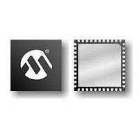
PIC16F1937-E/MV Microchip Technology, PIC16F1937-E/MV Datasheet - Page 150

PIC16F1937-E/MV
Manufacturer Part Number
PIC16F1937-E/MV
Description
14KB Flash, 512B RAM, 256B EEPROM, LCD, 1.8-5.5V 40 UQFN 5x5x0.5mm TUBE
Manufacturer
Microchip Technology
Series
PIC® XLP™ 16Fr
Datasheet
1.PIC16F1937-EMV.pdf
(472 pages)
Specifications of PIC16F1937-E/MV
Processor Series
PIC16F
Core
PIC
Program Memory Type
Flash
Program Memory Size
14 KB
Data Ram Size
256 B
Interface Type
MI2C, SPI, EUSART
Number Of Timers
5
Operating Supply Voltage
1.8 V to 5.5 V
Maximum Operating Temperature
+ 125 C
Mounting Style
SMD/SMT
Package / Case
UQFN-40
Development Tools By Supplier
MPLAB IDE Software
Minimum Operating Temperature
- 40 C
Core Processor
PIC
Core Size
8-Bit
Speed
32MHz
Connectivity
I²C, LIN, SPI, UART/USART
Peripherals
Brown-out Detect/Reset, LCD, POR, PWM, WDT
Number Of I /o
36
Eeprom Size
256 x 8
Ram Size
512 x 8
Voltage - Supply (vcc/vdd)
1.8 V ~ 5.5 V
Data Converters
A/D 14x10b
Oscillator Type
Internal
Operating Temperature
-40°C ~ 125°C
Lead Free Status / Rohs Status
Details
- Current page: 150 of 472
- Download datasheet (5Mb)
PIC16(L)F1934/6/7
REGISTER 12-22: WPUE: WEAK PULL-UP PORTE REGISTER
TABLE 12-12: SUMMARY OF REGISTERS ASSOCIATED WITH PORTE
DS41364E-page 150
bit 7
Legend:
R = Readable bit
u = Bit is unchanged
‘1’ = Bit is set
bit 7-4
bit 3
bit 2-0
Note 1:
ADCON0
ANSELE
CCPxCON
LATE
LCDCON
LCDSE2
PORTE
TRISE
WPUE
Legend:
Note 1:
Name
U-0
—
2:
2:
3:
Global WPUEN bit of the OPTION_REG register must be cleared for individual pull-ups to be enabled.
The weak pull-up device is automatically disabled if the pin is in configured as an output.
x
These bits are not implemented on the PIC16(L)F1936 devices, read as ‘0’.
Unimplemented, read as ‘1’.
These registers/bits are not implemented on PIC16(L)F1936 devices, read as ‘0’.
= unknown,
Unimplemented: Read as ‘0’
WPUE: Weak Pull-up Register bit
1 = Pull-up enabled
0 = Pull-up disabled
Unimplemented: Read as ‘0’
LCDEN
SE23
Bit 7
—
—
—
—
—
—
U-0
PxM<1:0>
—
u
= unchanged,
SLPEN
SE22
Bit 6
—
—
—
—
—
W = Writable bit
x = Bit is unknown
‘0’ = Bit is cleared
U-0
—
– =
WERR
SE21
Bit 5
—
—
—
—
—
unimplemented locations read as ‘0’. Shaded cells are not used by PORTE.
DCxB<1:0>
CHS<4:0>
U-0
—
SE20
Bit 4
—
—
—
—
—
—
U = Unimplemented bit, read as ‘0’
-n/n = Value at POR and BOR/Value at all other Resets
R/W-1/1
WPUE3
WPUE3
SE19
Bit 3
RE3
—
—
—
(2)
CS<1:0>
TRISE2
ANSE2
LATE2
RE2
SE18
Bit 2
—
CCPxM<3:0>
(1)
(1)
U-0
(1)
(1)
—
2008-2011 Microchip Technology Inc.
GO/DONE
TRISE1
ANSE1
LATE1
RE1
SE17
Bit 1
—
LMUX<1:0>
(1)
(1)
(1)
(1)
U-0
—
TRISE0
ANSE0
LATE0
ADON
RE0
SE16
Bit 0
—
(1)
(1)
(1)
(1)
Register
on Page
U-0
—
163
149
234
149
329
333
148
148
150
bit 0
Related parts for PIC16F1937-E/MV
Image
Part Number
Description
Manufacturer
Datasheet
Request
R

Part Number:
Description:
IC, 8BIT MCU, PIC16F, 32MHZ, SOIC-18
Manufacturer:
Microchip Technology
Datasheet:

Part Number:
Description:
IC, 8BIT MCU, PIC16F, 32MHZ, SSOP-20
Manufacturer:
Microchip Technology
Datasheet:

Part Number:
Description:
IC, 8BIT MCU, PIC16F, 32MHZ, DIP-18
Manufacturer:
Microchip Technology
Datasheet:

Part Number:
Description:
IC, 8BIT MCU, PIC16F, 32MHZ, QFN-28
Manufacturer:
Microchip Technology
Datasheet:

Part Number:
Description:
IC, 8BIT MCU, PIC16F, 32MHZ, QFN-28
Manufacturer:
Microchip Technology
Datasheet:

Part Number:
Description:
IC, 8BIT MCU, PIC16F, 32MHZ, QFN-28
Manufacturer:
Microchip Technology
Datasheet:

Part Number:
Description:
IC, 8BIT MCU, PIC16F, 32MHZ, SSOP-20
Manufacturer:
Microchip Technology
Datasheet:

Part Number:
Description:
IC, 8BIT MCU, PIC16F, 20MHZ, DIP-40
Manufacturer:
Microchip Technology
Datasheet:

Part Number:
Description:
IC, 8BIT MCU, PIC16F, 32MHZ, QFN-28
Manufacturer:
Microchip Technology
Datasheet:

Part Number:
Description:
IC, 8BIT MCU, PIC16F, 20MHZ, MQFP-44
Manufacturer:
Microchip Technology
Datasheet:

Part Number:
Description:
IC, 8BIT MCU, PIC16F, 20MHZ, QFN-20
Manufacturer:
Microchip Technology
Datasheet:

Part Number:
Description:
IC, 8BIT MCU, PIC16F, 32MHZ, QFN-28
Manufacturer:
Microchip Technology
Datasheet:

Part Number:
Description:
MCU 14KB FLASH 768B RAM 64-TQFP
Manufacturer:
Microchip Technology
Datasheet:

Part Number:
Description:
7 KB Flash, 384 Bytes RAM, 32 MHz Int. Osc, 16 I/0, Enhanced Mid Range Core, Low
Manufacturer:
Microchip Technology

Part Number:
Description:
14KB Flash, 512B RAM, 256B EEPROM, LCD, 1.8-5.5V 40 UQFN 5x5x0.5mm TUBE
Manufacturer:
Microchip Technology


