MICRF405YML TR Micrel Inc, MICRF405YML TR Datasheet - Page 33
MICRF405YML TR
Manufacturer Part Number
MICRF405YML TR
Description
868-915 MHz ISM Band Transmitter
Manufacturer
Micrel Inc
Datasheet
1.MICRF405YML_TR.pdf
(46 pages)
Specifications of MICRF405YML TR
Frequency
290MHz ~ 980MHz
Applications
ISM
Modulation Or Protocol
ASK, FSK
Data Rate - Maximum
200 kbps
Power - Output
10dBm
Current - Transmitting
18mA
Data Interface
PCB, Surface Mount
Antenna Connector
PCB, Surface Mount
Voltage - Supply
2.2 V ~ 3.6 V
Operating Temperature
-40°C ~ 125°C
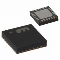
Package / Case
24-MLF®, QFN
Operating Temperature (min)
-40C
Operating Temperature (max)
125C
Operating Temperature Classification
Automotive
Product Depth (mm)
4mm
Product Length (mm)
4mm
Operating Supply Voltage (typ)
2.5/3.3V
Operating Supply Voltage (max)
3.6V
Lead Free Status / RoHS Status
Lead free / RoHS Compliant
Features
-
Memory Size
-
Lead Free Status / Rohs Status
Compliant
Other names
576-1965-2
MICRF405YMLTR
MICRF405YMLTR
MICRF405YMLTR
MICRF405YMLTR


April 2006
Low Dropout Regulator (LDO) and Low Battery Detector
The MICRF405 has three internal LDOs powering
up different parts of the circuit, as can be seen in the
Block Diagram. The output voltages of the LDOs are
around 2.4V. The LDOs can be turned off (default
setting is on) by setting the LDO_en[1:0]=0.
When LDO_en[1:0]=3, the power supply range is
2.2-3.6 volt. Power must be applied to pin 1 and 11.
A capacitor is needed on each of the LDO output for
stability (pin 3, 9 and 23). In sleep mode, all the
LDOs are turned off. The interface and control
blocks run on unregulated power, meaning that the
register
programming can also be done in this mode.
An option, where the LDOs are bypassed, is
enabled by setting the LDO_by bit, and when
activated, the transmitter can operate at 2.2V-2.5V.
Since the LDO drop is decreased, the output power
is slightly higher. However, in this mode it is of vital
importance that the input power is below 2.5V as the
pass devices in the LDOs are fully on and not
regulated. It is recommended that this option is used
in combination with the low battery detector.
When LDO_en[1:0]=0, the power supply range is
2.2-2.5 volt. Power must be applied to pin 1, 3, 9, 11
and 23. Capacitors are now only needed for normal
0001011
0001100
A6..A0
Adr
LowBatt_level=0
content
LowBatt_en=1
D7
will
Freq_Band1=0
LDO_by=0
be
D6
kept
Freq_Band0=1
and
LDO_en1=1
D5
that
the
VCO_freq2=0
LDO_en0=1
D4
33
Data
noise decoupling. Alternatively, connect power to
pins 1 and 11 only, and set LDO[1:0]=3 and
LDO_by=0.
The LDOs are controlled with 2 bits, enabling the
option of running the complete circuit on the RF LDO
alone (LDO_en[1:0]=1), or on the RF LDO and
analog LDO (LDO_en[1:0]=2). Doing so, regulated
power on the RFVDD pin must be externally routed
to the AVDD and DVDD pin in the first case and,
and from the RFVDD to the DVDD pin in the second
case. These modes will save one or two of the
external capacitors used for stabilizing the LDOs,
but might influence the phase noise and spurious
performance. Recommended use is therefore,
LDO_en[1:0]=3 or 0.
The low battery detector circuit is turned on when
the LowBatt_en bit is set. It will monitor the voltage
of the input power, pin 11, in standby and TX
modes. If LDO_by=0, it will set the LowBatt interrupt
if the voltages falls below 2.1V for LowBatt_level=1
and 2.0V for LowBatt_level=0. If LDO_by=1, it sets
the interrupt when the voltages is below 1.9V/1.8V
for LowBatt_level=1/0.
MOD_LDc_en=0
VCO_freq1=1
D3
PA_FEc_en=0
VCO_freq0=1
D2
Modulation1=1
PA_LDc_en=0
D1
Modulation0=0
(408) 955-1690
M9999-041906
LD_en=1
D0
Related parts for MICRF405YML TR
Image
Part Number
Description
Manufacturer
Datasheet
Request
R

Part Number:
Description:
MICRF405 Eval Board For Experimental Use Only
Manufacturer:
Micrel Inc
Part Number:
Description:
MICRF405 Eval Board For Experimental Use Only
Manufacturer:
Micrel Inc
Part Number:
Description:
MICRF405 Eval Board For Experimental Use Only
Manufacturer:
Micrel Inc
Part Number:
Description:
MICRF405 Eval Board For Experimental Use Only
Manufacturer:
Micrel Inc
Part Number:
Description:
Manufacturer:
Micrel Inc
Datasheet:
Part Number:
Description:
Manufacturer:
Micrel Inc
Datasheet:
Part Number:
Description:
Manufacturer:
Micrel Inc
Datasheet:
Part Number:
Description:
Manufacturer:
Micrel Inc
Datasheet:
Part Number:
Description:
Manufacturer:
Micrel Inc
Datasheet:
Part Number:
Description:
Manufacturer:
Micrel Inc
Datasheet:
Part Number:
Description:
Manufacturer:
Micrel Inc
Datasheet:
Part Number:
Description:
Manufacturer:
Micrel Inc
Datasheet:
Part Number:
Description:
Manufacturer:
Micrel Inc
Datasheet:
Part Number:
Description:
Manufacturer:
Micrel Inc
Datasheet: