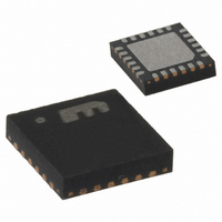
MICRF405YML TR Micrel Inc, MICRF405YML TR Datasheet - Page 27

MICRF405YML TR
Manufacturer Part Number
MICRF405YML TR
Description
868-915 MHz ISM Band Transmitter
Manufacturer
Micrel Inc
Datasheet
1.MICRF405YML_TR.pdf
(46 pages)
Specifications of MICRF405YML TR
Frequency
290MHz ~ 980MHz
Applications
ISM
Modulation Or Protocol
ASK, FSK
Data Rate - Maximum
200 kbps
Power - Output
10dBm
Current - Transmitting
18mA
Data Interface
PCB, Surface Mount
Antenna Connector
PCB, Surface Mount
Voltage - Supply
2.2 V ~ 3.6 V
Operating Temperature
-40°C ~ 125°C
Package / Case
24-MLF®, QFN
Operating Temperature (min)
-40C
Operating Temperature (max)
125C
Operating Temperature Classification
Automotive
Product Depth (mm)
4mm
Product Length (mm)
4mm
Operating Supply Voltage (typ)
2.5/3.3V
Operating Supply Voltage (max)
3.6V
Lead Free Status / RoHS Status
Lead free / RoHS Compliant
Features
-
Memory Size
-
Lead Free Status / Rohs Status
Compliant
Other names
576-1965-2
MICRF405YMLTR
MICRF405YMLTR
MICRF405YMLTR
MICRF405YMLTR
April 2006
Modulation
The frequency modulation can be done in three
different ways with the MICRF405, either by closed-,
open loop VCO modulation or by modulation with
the internal dividers. Amplitude modulation can also
be done in two different ways, either ASK/OOK or
Spread Spectrum ASK™. All these different types of
modulation is selected by Modulation1-0 and
ASK_en (See chapter bit description for details).
Closed loop VCO modulation (Modulation[1:0]=0),
the modulation is applied directly to the VCO. The
PLL will see the modulation as a frequency error and
try to tune the VCO back to carrier. The PLL
bandwidth therefore, needs to be sufficiently low
enough not to cancel the modulation (at least 20
times lower than the slowest variation of the
modulation). Also, the modulation needs to be DC-
free, usually by encoding the data by a DC-free code
such as Manchester or 3b4b. In most cases, an
external PLL loop filter must be used to fulfill the
demand for low bandwidth. Please see the
Modulator section for details on deviation and
shaping.
Open Loop VCO Modulation (Modulation[1:0]=1),
modulation is applied directly to the VCO. The VCO
is now left free-running. The varactor voltage will
now be stored on a large external capacitor
connected to the VARIN pin and the PLL is disabled
during the modulation. With the PLL disabled, the
modulation will not be canceled and the modulated
data signal may include DC-components. The
switching between PLL active and disabled is done
automatically by checking the DATAIN pin. If it is tri-
stated the PLL is active, and if it is either high or low
or transitioning between high or low the PLL is then
disabled and the data on the DATAIN pin is
transmitted. When data is transferred through the
SPI the PLL is disabled during the transmission of a
packet, while enabled else. In this mode, the PLL
bandwidth can be fairly high as it is disabled during
transmission. However, due to the large external
capacitor, C3 in Figure 11b), the bandwidth is limited
due to the pole created by this capacitor. Both
internal with 56° phase margin and external filters
Micrel
0001011
0001110
0001111
0010000
0010001
0010010
A6..A0
Adr
VCO_Fr_Chk=0
MOD_TEST1=0
ASK_PN_en=0
LowBatt_en=1
Mod_I4=0
ASKn1=1
D7
VCO_Fr_Auto=0
Prescaler_Sel=0
Freq_Band1=0
ASK_EN=0
Mod_I3=1
ASKn0=0
D6
Freq_Band0=1
ASKshape2=1
ASKClk_K5=1
FSKClk_K5=1
Mod_I2=0
FSKn2=1
D5
FSKClk_K4=1
ASKshape1=1
ASKClk_K4=1
VCO_freq2=0
Mod_I1=0
FSKn1=0
D4
27
Data
are suitable. A high quality capacitor of 10-47nF
(COG type) should be connected on pin VARIN-to-
ground to ensure minimum frequency drift due to
leakage and frequency drift caused by the capacitor
dielectric relaxation phenomenon (25kHz offset after
50ms). For deviation and shaping, please see the
Modulator section. The frequency drift (Hz/ms) over
temperature due to leakage is shown in Figure 12
with a 33nF COG external capacitor.
Figure 13 shows the frequency drift in open loop
VCO
relaxation. The drift is around 40kHz during a time
period of 50ms. Of the 40kHz drift, 5-10kHz is due to
an initial offset caused by the modulator itself.
Date: 11.JAN.2006
1 AP
CLRWR
Figure 12. Frequency Drift Due to Capacitor Dielectric
ASKshape0=1
ASKClk_K3=0
FSKClk_K3=0
VCO_freq1=1
Ref
Center 915.00004 MHz
Mod_I0=1
FSKn0=0
160k
120k
80k
40k
0
-40k
-80k
-120k
-160k
-200k
-240k
D3
0 Hz
modulation
10:10:03
FSKClk_K2=1
ASKClk_K2=1
VCO_freq0=1
Relaxation at 915MHz.
Mod_A2=0
Mod_F2=1
ASK2=1
*
Att
D2
due
30 dB
10 ms/
to
Modulation1=1
ASKClk_K1=0
FSKClk_K1=0
IFB 10 MHz
AQT 100 ms
Mod_A1=1
Mod_F1=0
ASK1=1
capacitor
D1
MICRF405
Modulation0=0
FSKClk_K0=0
ASKClk_K0=0
(408) 955-1690
M9999-041906
Mod_A0=1
Mod_F0=0
ASK0=1
dielectric
D0
TRG
A


